

2005 Articles
The Boundary Scan Infrastructure
A primer on how boundary scan, or JTAG, works.
Boundary scan or, more accurately, the IEEE 1149.1 Standard Boundary Scan Test Strategy, traces its roots to the mid 1980s. That’s when an ad hoc working group, the Joint Test Action Group (hence the JTAG name for the methodology), began working on concepts for a circuit board test technology that would not require physical contact between a probe and a circuit board.
Several trends pointed to the disappearance of physical access for test probes. Device packages that were new at the time (like ball grid arrays) placed device pins under the silicon. As a result, probes could not be applied to the pins. Moreover, additional functionality was being packed onto circuit boards at a time when the size of the boards themselves was shrinking. Something had to give; most often, test points or test pads were eliminated from boards to save real estate. At the same time, multilayer boards increased the difficulties of physically accessing chip-to-chip interconnect nets below the surface layer of the board.
Out of this context the JTAG group began forming a boundary scan test strategy. The eventual solution centered on the concept of embedding an internal shift register around the perimeter of semiconductor devices, a boundary scan register.
At the chip level, a component is defined as a boundary scan device when each primary input and output signal is supplemented with a multi-purpose memory element called a boundary scan cell (Figure 1). A board’s collection of boundary scan cells is configured into a parallel-in, parallel-out shift register by way of a four-wire interface. This scan path, as it is called, is made up of test data in (TDI), test clock (TCK), test mode select (TMS) and test data out (TDO) signals. A fifth signal, test reset (TRST) is optional. Collectively these device pins are known as the test access port (TAP). Data can be shifted into and out of the scan chain connecting the boundary scan cells on multiple devices on a board. Because of these capabilities, boundary scan cells can be thought of as virtual nails because they are able to set up and apply tests across the interconnect structures on the board.
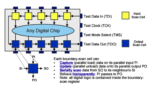 |
| FIGURE 1: Boundary scan cells. |
Devices that do not have embedded boundary scan cells can still be tested by boundary scan. A JTAG device directly connected to a non-boundary scan device can drive signals onto the non-boundary scan device and test its interconnects in this way.
Test Development
Before a boundary scan test pattern can be automatically generated by a test system (see Figure 2 for the configuration of a typical boundary scan test or programming station), boundary scan devices on the board and the scan path must be characterized. The test development station does this by examining the board netlist and compiling a database with files that describe the boundary scan devices in boundary scan description language (BSDL). BSDL is defined in the IEEE 1149.1 standard. A device’s BSDL file describes all the boundary scan features of the device.
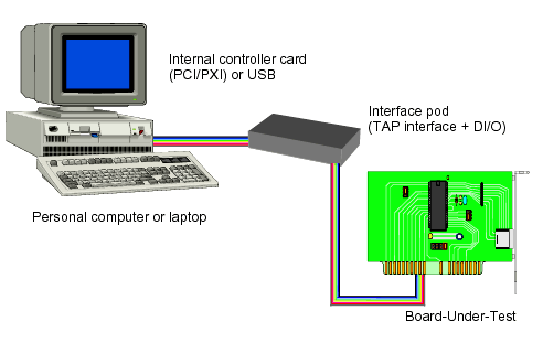 |
| FIGURE 2: Typical boundary scan test or programming station. |
Non-boundry scan devices to be tested must also be characterized in the design’s database. Online libraries of models that describe non-boundary scan devices can be automatically downloaded by the test generation system and included in the database to extend the reach of JTAG tests to non-boundary scan devices.
As part of the test generation process, advanced boundary scan test systems will generate fault coverage reports that indicate how much test coverage can be derived from the information provided in a database. The user can then decide whether more information should be provided or certain steps to take to increase test coverage.
Following the application of test patterns, a test results report is generated. Diagnostic tools included in the more advanced JTAG systems can isolate faults or defects down to the level of a particular pin on a device.
Access provided by boundary scan can also be used to load data or software into programmable logic devices (PLDs) or memory after these devices have been soldered onto a board. This in-system programming or in-system configuration capability eliminates the need to remove devices from boards to load new versions of firmware or software. Even after a system has been installed, firmware updates can be loaded into PLDs via boundary scan.
Test Reuse
A major benefit of boundary scan technology is the portability of testing and programming operations. For example, tests developed during a system’s design phase to debug prototypes can migrate with the system as it moves into manufacturing, where the same tests can be applied by a benchtop JTAG manufacturing station or combined with other tests on an in-circuit test (ICT) platform. Seamless integration of a full-blown boundary scan system on an ICT system offers significant cost savings by eliminating the need to redevelop boundary scan tests from the development department and the coverage supplied by JTAG tests will simplify ICT tests, cutting the cost of fixtures and the time to produce them.
Boundary scan tests can also migrate with a system into the field where they can be used to troubleshoot malfunctions or to load new versions of embedded irmware.
The engineers who developed the IEEE 1149.1 standard more than a decade ago might be surprised by today’s applications of this technology. Boundary scan has branched out beyond its roots as a test methodology for shorts and opens.
Several new IEEE standards and at least one proprietary embedded test methodology depend upon the JTAG infrastructure. The IEEE 1149.6 Boundary Scan Standard for Advanced Digital Networks, for example, uses scan chains to test high-speed serial buses such as Gigabit Ethernet and Fibre Channel. In addition, the IEEE 1532 Standard for In-System Configuration is based on boundary scan access to PLDs. Multiple PLDs can be configured concurrently with IEEE 1532, reducing programming times considerably. Also, Intel recently delivered a JTAG-based embedded test technology known as interconnect built in self test (IBIST). IBIST will be included in many of Intel’s future chips to lower the overall cost of test and more effectively validate high-speed buses.
David Bonnett is technical manager, ASSET InterTech Inc. (asset-intertech.com); dbonnett@asset-intertech.com.


Press Releases
- Seika Machinery’s SMI 2026 Webinar Series Continues with Focus on PCB Cleaning Before Solder Paste Printing
- Forwessun Expands Testing Capabilities through Strategic TRI Alliance
- Federal Electronics Expands Advanced Manufacturing Capabilities to Support Military and Aerospace Cable Assembly and Wire Harness Programs
- Altus Continues Irish Growth with Expansion of Engineering Team