

2005 Articles
How Post-Print Inspection Improves Performance
The skinny on how AOI and integrated systems add up.
Due to the complexity of the variables associated with solder paste printing, the vast majority of defect opportunities originate with this process step. The defect rate of the manufacturing process is an important metric to monitor – it determines how the process line is actually performing. Most assemblers will measure the performance of the entire process by counting the number of defect opportunities on an assembly and then monitor the number of defects actually produced. Comparing the number of actual defects produced versus the number of opportunities will determine the actual process performance in parts per million (PPM) or defects per million opportunities (DPMO).
A defect opportunity is often calculated one for each solder joint and one for the component itself. For example, a 208-pin quad flatpack would have a total of 209 defect opportunities: 208 from the solder joints and one for the component. Typical defects include misplaced, incorrect polarity, missing and non-functioning components.
Solder paste printing and soldering processes can account for more than 80% of defect opportunities. Even a small improvement in the printing process will result in a dramatic improvement in the quality of the entire SMT manufacturing process.
One of the primary tools to understand printing performance is the inspection and evaluation of the printed solder. This process step is commonly called post-print inspection. A significant benefit of post-print inspection is the dramatic cost reduction to repair the identified defects. Several studies have demonstrated the correlation between costs to repair a defect in relation to where in the process the defect is discovered. A printing defect detected immediately after printing can be corrected at small cost while a printing defect that results in a product failure at a customer site can cost several thousands times more.
Post-print inspection systems have been available for years and come integrated into the printer or as a dedicated, separate piece of inspection equipment. A post-print solder paste inspection system should evaluate three primary regions of interest. The first quantifies how much of the board pad is covered by paste. Second is the space (gap) between pads. Evaluating the amount of paste between the pads is commonly called bridge detection. Third is the inspection of the stencil, which will identify paste buildup between apertures and can initiate a stencil wipe when buildup exceeds acceptable limits.
Post-print inspection systems integrated into the printer have the distinct advantage of having access to the stencil and can include all three regions of interest. However, for most available printers, the machine cannot perform any other functions during the post-print inspection process. This sequential processing limits the throughput of the line and reduces the number of manufacturers that take advantage of full post-print inspection. AOI systems are located after the printer and have the advantage of performing post-print inspection without slowing printing cycle time. However, AOI does not have access to the stencil. This limits AOI inspection to board pad coverage and the evaluation of the space between pads. Figure 1 illustrates the process of inspecting PCBs.
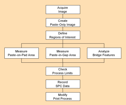 |
| FIGURE 1: PCB inspection process. |
Initially the board image is acquired either by an area or line scan camera. The acquired image is processed so the areas covered with solder can be identified. Various analysis techniques are used to evaluate the presence of solder in the regions of interest. The resulting measurements are compared to user-defined process limits. Historical data are used to monitor trends.
The paste detection process is used to describe an image processing method in which solder is separated from non-paste features. This creates a paste-only image that can be used to evaluate print quality. Solder paste detection methods include direct application of single or dual thresholds to the captured image, image subtraction techniques, and texture-based substitution. All methods are intended to separate paste from non-paste regions.
The most common techniques are based on single or dual threshold methods that use pixel brightness to isolate solder paste regions. A single threshold, or brightness level, is chosen to create a binary image depicting paste and non-paste regions. Dual threshold methods work similarly but include a scalable transition region of brightness levels between thresholds to more accurately account for edge pixels. The transition region is preferred since small paste features can contain a relatively significant amount of edge data.
Subtraction methods create a different image by subtracting one image from another. Subtraction methods typically compare differences between a reference image and a newly captured image to detect paste. The images must be registered precisely to each other to minimize error. It is difficult to use either of these methods to separate paste from the background images when brightness levels overlap.
Finally, a third method for detecting solder paste uses texture-based recognition. This method performs a combination of mathematical and morphological operations on a digitized image to separate areas of solder paste texture from other dissimilarly textured non-paste areas on a PCB, stencil, wafer or substrate. Using texture-based recognition removes potential issues that result from brightness overlap.
Joe Belmonte is project manager, advanced process development, at Speedline Technologies (speedlinetech.com); jbelmonte@speedlinetech.com.


Press Releases
- Changes in Incap’s Management Team: Incap updates its leadership model to support its growth strategy
- Niche Electronics Celebrates Completion of Florida Expansion
- Microscreen Names Nik Thomas Director, Expands Leadership Role Amid Continued Organizational Growth
- W&S Enters New Growth Phase Through Strategic Partnership and New Leadership