

2005 Articles
3-D Packaging Gets Ready for Prime Time
Among the benefits: improved RC delay and power consumption.
Driven by portable applications that require extremely small form factors, shipments of stacked die packages will exceed a billion units in 2005. With mobile phones, digital camcorders and cameras containing at least one stacked die CSP in each product, this form of stacked die packaging has definitely arrived. But what about the stacking of wafers? When will such technology be commercialized? What will drive its development?
3-D packaging is not a new concept. Many companies have been stacking packages (mainly memory) for years and continue to expand their product offerings. These companies include Irvine Sensors, Staktek, 3-D Plus and Vertical Circuits. 3-D Plus uses flex circuits to mount the die before stacking and has created structures for use in military/aerospace, industrial and medical applications. Staktek, famous for its stacked TSOPs, has introduced a new method using flex circuit that includes the stacking of logic devices. Tessera’s folded stacking technology is also based on the use of two-metal layer flex circuit and has been adopted by Intel.
Advantages of stacked solutions include smaller form factor, fast turn-time and low non-recoverable engineering costs (compared to a single die design). While most stacked die packages shipped have historically contained memory (flash and SRAM), packages containing logic devices are also moving into production. Today’s packages typically contain as many as four or five die, but packages with eight to 10 die have been introduced in prototype quantities by Fujitsu, Intel, STMicroelectronics and Toshiba. The die in some of these stacks have been thinned to 50 µm. The majority of packages shipping today are wire bonded, but flip chip is on the roadmaps of semiconductor makers and IC package contract assembly houses. Flip chip is often in the form of gold stud bump bonding because it permits fine pitches (as fine as 80 µm).
Challenges for stacked die products include logistical and engineering issues. Issues related to stacked die include wafer thinning, bare die, known good die (KGD), die attach and wire bond, and thermal dissipation. Concerns about KGD and the logistics of purchasing bare die have resulted in a plethora of package constructions that feature packaging stacking – either alone or in conjunction with bare die stacking.
Short vertical interconnections. International Sematech’s International Technology Roadmap for Semiconductors (ITRS) has identified 3-D IC stacking as the way to achieve further improvements in silicon IC performance. Driven by the need for improved performance, a number of companies are researching methods to use short vertical interconnections to replace the long interconnects found in 2-D structures. According to Intel, 3-D interconnects improve RC delay and power consumption by reducing wiring lengths. The density of the structure would provide not only improved performance, but also a dense solution that permits a smaller form factor. Stacking disparate technologies to provide a structure with potential functions including logic, memory, MEMS, antennas, display, RF, analog/digital, sensors and power storage is potentially possible with 3-D heterogeneous integration, making this technology the Holy Grail of system integration.
The new 3-D options include both wafer-to-wafer stacking and chip-to-wafer stacking. Many universities have research programs, including Albany Nanocenter, Arkansas, Delft, Hong Kong University of Science and Technology, MIT, RPI and Tohoku University. Research institutes and consortia developing these methods include the Fraunhofer IZM in Berlin and Munich, IME in Singapore, IMEC in Belgium, Lincoln Labs and MCNC-RDI in the U.S. ASET, the Japanese consortium, concluded its research activities in 2004 and has already seen the formation of one spinout company, ZyCube. Companies including Infineon, Intel, IBM, Matrix Semiconductor, Micron, Oki, Samsung, Renesas Technology, Tezzaron, Toshiba and Ziptronix have research activities.
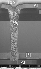
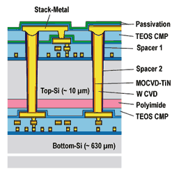
Key in the development of the technology is the use of through wafer vias (Figure 1), wafer thinning and the ability to bond these new structures. Through wafer via options include deep etch capability such as the anisotropic “Bosch etch.” Innovative solutions are being developed by a number of companies and include insulator formation by CVD TEOS or polymers. Conductor options include copper, tungsten or poly silicon. Wafer thinning features lapping/grinding followed by wet etch, plasma etch or CMP. Bonding options include silicon or metal fusion, CuSn eutectic, polymer bonding and bumping. Companies such as Silicon Genesis Corp. and Ziptronix have demonstrated novel room temperature bonding methods.
 |
 |
| FIGURE 1: Photo (left) and drawing (right) showing through via concept. | |
While a number of companies are investigating wafer stacking for a variety of device types, the first applications for wafer-to-wafer stacking are likely to be memory products. Oki, a participant in the ASET consortium, shows stacked memory on its roadmap after 2007. Tezzaron, using the MagnaChip (formerly Hynix) facility in Korea, is focusing on SRAMs and DRAMs. The company is sampling DDR2 and is targeting the mobile phone market. ZyCube’s first demonstration product is an image sensor where a glass cap is formed over a sensory circuit while interconnects are formed through the wafer. With chip-to-wafer stacking a number of combinations are under investigation including memory and logic. Renesas and Hitachi have demonstrated microprocessor and SDRAM chip stacking structures using the through-hole vias at temperatures less than 150°C, wafer thinning down to >30 µm and laser wafer dicing.1
Stacked die package shipments continue to grow and the number of die inside each package is increasing. Stacked die packages containing both memory and logic are now common. The growth in stacked packages is driven by the need to incorporate greater functionality into smaller areas. Coupled with increased performance, these needs have driven the development of novel 3-D packaging structures. Innovation will continue the drive of new equipment, materials and process development. The future of this technology is one of the most exciting new developments in the industry today.
Reference
- N. Tanaka, et al., “Ultra-Thin 3-D-stacked SIP formed Using Room-Temperature Bonding between Stacked Chips,” Electronic Components and Technology Conference Proceedings, June 2005, pp. 788-794.
E. Jan Vardaman is president of TechSearch International, Austin, TX; jan@TechSearchInc.com. Her column appears semimonthly.


Press Releases
- Incap Germany Receives Strong Defense Orders from KNDS for Leopard Tank Program
- Altus Group Partners with Optimum to Bring Smart Klaus Digital Assembly Technology to UK and Ireland
- Heller Industries Strengthens Global Customer Focus with Appointment of Senior Key Account Manager Mike DePauw
- Amtech Electrocircuits Launches First Article to Deliver Practical AI Insights for Hardtech Manufacturers