

2005 Articles
Practical Pb-Free Implementation
A review of six major considerations, from equipment choice to process validation.
The transition to Pb-free electronics is becoming reality. The RoHS and WEEE regulations, although still with a number of implementation questions, have final implementation dates. Many electronics manufacturers have some Pb-free process capacity; others are making a significant effort to learn what is required, and some are in the beginning stages of understanding the Pb-free process.
Numerous scientific studies have been published regarding Pb-free concerns: equipment capability, solder alloy types, component metalization, process chemistries, PWB materials and surface finishes. Scientists and engineers have demonstrated feasibility, and some parts of the world are engaged in full-scale production of Pb-free electronics. But many assemblers, particularly those in North and South America, are still formulating their transition plan. The scientific work that identified Pb-free solutions must now be translated into practice on the shop floor. This is a considerable undertaking, given all the variables that exist in a production environment. This article provides the framework for planning the transitions of individual factories. It combines the experience of several engineers who have supported Pb-free transitions around the world.
Step 1: Equipment. Verify that production equipment in the factory is capable of supporting Pb-free materials. Consider all the equipment in a production facility. Obvious equipment considerations include the hot processes such as reflow and wave soldering. Less obvious are the data-logging devices; rework systems, solder pallets, cooling apparatus and other assembly equipment.
First, verify that the oven data logger can operate at higher temperatures. It may need a better-insulated protective case. This is easily verified by calling the device’s manufacturer.
Once the capability of the data logger used to create heating profiles (recipes) for the reflow and wave soldering processes is verified, check the heating and cooling capability of the soldering systems. The most difficult to profile board under SnPb temperatures is likely the most difficult to profile under Pb-free temperatures also. Situations with large delta T’s will probably require longer soak zones and perhaps longer times above liquidus (TALs). Peak temperatures and TALs will be traded off in the profiling process. Early profiling is important to understand equipment capability, and to aid in selecting solder pastes and other materials later in the implementation process.
Some tricks to achieving appropriate profiles include the “reverse spike” and “double spike” recipes. In the reverse spike scenario (Figure 1), the second-to-last zone is used for the spike, and the last zone is set below spike temperatures. The double spike recipe, sometimes seen in 10-zone SnPb processes, simply uses the last two zones to spike, at equal but lower setpoints. These recipes help control high peak temperatures while trying to achieve recommended TAL on thermally challenging boards.
 FIGURE 1: Reverse spike reflow profile may help some assemblies achieve good TALs without exceeding peak temperatures.
 |
After passing through the chip wave, solder joints cool and begin to solidify. When they reach the smooth wave, they are reheated and re-melted. Once the solder again becomes molten, its wetting forces can act on the lead and the barrel to fill the hole. The shorter distance between nozzles gives the Pb-free solder less time to cool, and requires less energy to re-melt the solder in the barrels, thus providing more contact time on the smooth wave for wetting. The net result of closer nozzles is better hole fill (Figures 2-4).
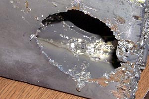 FIGURE 2: Stainless steel flow duct corroded by Sn-rich solder alloy. Stainless steel will degrade after six to 12 months exposure to Pb-free solder.
 |
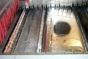 FIGURE 3: Typical SnPb wave solder nozzle for air environment. Note the distance between waves.
 |
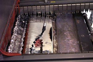 FIGURE 4: Pb-free wave solder nozzle for air environment. Note the shorter distance between waves.
 |
Thermal profiles comparing the two nozzle types can be seen in Figure 5. Solid traces represent Pb-free nozzles; dashed traces represent SnPb nozzles. Both were processed at Pb-free temperatures (250°C) without preheat. Notice the dramatic difference in joint temperatures with the closer nozzles.
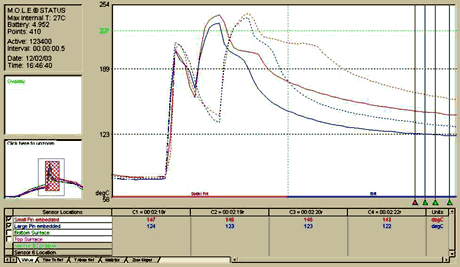 FIGURE 5: Thermal profiles for traditional tin-lead and lead-free nozzles. The Pb-free nozzles do not permit as much cooling between waves, resulting in better hole fill.
 |
Solder pot maintenance will have a few new considerations compared to SnPb soldering. Solder analysis should be performed more frequently to monitor the levels of lead (coming from components that are not yet Pb-free) and copper (coming from circuit boards). This is extremely important on selective solder or mini-wave machines, which have smaller pots that get saturated faster. Lead levels of greater than 0.1% limit the ability to define a solder joint as “Pb-free”1 and can also contribute to fillet lifting in through-hole devices. Copper levels greater than 0.9% can make tin and SAC alloys more sluggish, causing solder bridges. Removal of copper from the alloy also presents a new challenge, as the CuSn intermetallic compound is denser than tin, SnCu or SAC alloys, and cannot float to the top of the pot and be skimmed, as was the typical practice with SnPb. The lower density of Pb-free alloys also means that hand tools erroneously dropped into the solder pot will no longer float to the top.
If pallets are used in wave soldering, they should be part of the material considerations. Pallets will be exposed to longer thermal cycles with slower conveyor speeds and longer contact times in the wave. They may need more frequent cleaning. Check with the pallets’ supplier to verify the material’s stability, to see if they have any experience with Pb-free soldering the specific material or if protective coatings are available to prolong service life.
Rework stations will require verification also. Although most stations will be able to reach the proper temperatures, boards may become more difficult to profile. As with reflow, check both heavy and light boards to understand the process window and the higher temperature’s impact on warpage and handling. Component body temperature should also be monitored as the reflow temperature of the solder approaches the maximum allowable temperature of the component.
Soldering irons are located throughout the factory – at inspection stations, rework stations, test stations and sometimes final assembly. The location of all irons should be recorded, so that if new tips are needed they can be deployed to all appropriate places. These locations will also require spools of Pb-free solder, and operators and technicians will need to be trained on how to identify Pb-bearing from Pb-free products.
Pb-free solder paste’s printability will not change, but its spread during reflow will, which may require a tightening of the stencil printing process.
One concern is print accuracy, or the alignment of the printed solder paste to the circuit board pad. Because Pb-free alloys do not spread or wet as well as SnPb, any solder paste not accurately printed onto the PCB will stay close to where it was printed after reflow. Figures 6 and 7 depict the same deposits before and after reflow for QFPs and passives. The major concern is the accuracy of the printing equipment to align the stencil apertures to the PCB pads. When addressing the variation in stencil to PCB alignment, consider the variation of the positional accuracy of the PCB, variation of the alignment capability of the printer and variation in the stencil itself.2 If the variation of the stencil is contained, and the variation of a calibrated printer is known to be +/- 0.001" at Six Sigma,3 then the remaining factor is the positional accuracy of the PCB itself. PCB variation is the largest contributor to misalignment. PCBs are known to “shrink” from CAD data as a result of their fabrication process. They also experience some shrink in their first reflow process, exacerbating misalignment issues when printing the second side of the board.
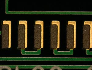 FIGURE 6: Pb-free QFP print after reflow. Note the lack of spread during reflow process. FIGURE 6: Pb-free QFP print after reflow. Note the lack of spread during reflow process. |
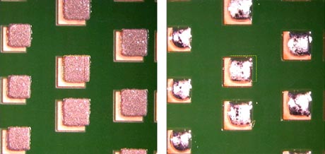 FIGURE 7: Pads for 0603 and 0805 components before and after reflow process. Again note the lack of spread. FIGURE 7: Pads for 0603 and 0805 components before and after reflow process. Again note the lack of spread. |
To address variation in the PCB, it can be measured and mapped; a stencil can be generated to custom-fit the PCBs. Generally, all boards in a manufacturing lot shrink by the same proportion if oriented in the same direction on the vendor panel. For large volume production, it is economically advantageous to request the board manufacturer to measure the boards and provide positional data so a customized stencil can be cut to match. The improvement in yields far offsets the cost of the stencil. Measuring and mapping the board brings the added benefit of programming the pick-and-place equipment with actual location data, thereby reducing defects typically associated with pick-and-place: misplacements, tombstones and solder balls or bridges that result from paste smears.4
Work has been performed to identify the optimum aperture for chip components (0402 – 1206) that will permit good pad coverage while limiting defects like mid-chip solder balls (MCSB) and tombstones.5 Three experimental apertures, shown in Figure 8, were compared to industry standard rectangular and home plate apertures.
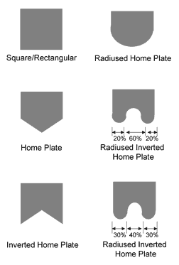 FIGURE 8: Experimental apertures designed for Pb-free paste printing.
 |
The final consideration in the assembly line is the placement system. With the exception of component vision files, Pb-free processing has little impact on the placement process. Components will have the same size and shape, but have a Pb-free finish on their leads or bumps. Finishes may include matte tin, SnCu, SnBi, SAC, NiPd or NiAu. Whatever finish is applied to the leads, it may appear differently to the vision processor than its SnPb predecessor. Depending on how a facility manages its vision files, the best option may be to test Pb-free devices as they become available and have separate files for SnPb and Pb-free components until the transition is complete.
Another area of concern is placement accuracy. Several formal studies, including one performed by Speedline Technologies, showed that component self-centering during reflow is not as robust in Pb-free processes.6 Components that will center on the board pads in a SnPb process will not do so as well in a Pb-free process. Placement processes should be monitored to ensure proper component orientation after reflow.
The majority of equipment considerations can be reviewed well in advance of running Pb-free processes. In fact, some of them must be reviewed in advance. Conversely, many can be performed without Pb-free materials, but others must wait until the Pb-free materials are available and in stock. Any preparation or evaluation that can be performed in advance will not only help smooth the transition, but certain aspects (like tightening stencil printers and placement machines) may also bring some immediate improvements to the current SnPb process.
Step 2: Investigate material compatibility. Obviously the solder paste will change when a Pb-free formulation is used. Factors influencing solder paste selection include: printability, stencil life, pin testability, tack, reflow window and joint cosmetics. Regardless of alloy, each assembler must determine which factors are most important to them and prioritize their selection accordingly. When moving to Pb-free solder paste, the difference in surface appearance should be considered early, as it will affect inspection and yields.
When evaluating a paste, reference the profiles generated in Step 1. Solder pastes under evaluation should be processed at similar times and temperatures. These assemblies can then be used to assess worst-case residue cosmetics (if no-clean) or cleanability (if water-soluble). If water-soluble paste is used, clean after each reflow pass; if this is not possible, check cleaning after two reflow cycles.
Long, hot thermal excursions present a worst-case scenario for flux residues. Fast, cool thermal excursions present a worst-case scenario for solder joint cosmetics. An assembly should also be tested under an anticipated fast thermal excursion, using a shorter time above liquidus and lower peak temperature. This assembly can then be assessed for wetting, surface appearance and fusion of fine features.
Will the current wave flux be compatible with Pb-free alloys in wave soldering? It could be, depending on the vintage of the formulation. Most liquid fluxes developed in the past few years are likely to work well with Pb-free solders. The manufacturer probably tested the flux with Pb-free solders during its development.
If a more mature flux formulation is used, the likelihood of Pb-free compatibility is lower. A water-soluble flux is more likely to stand up to the demands of a Pb-free process than a no-clean, which is designed to become benign after the thermal exposure of a SnPb process. Check with the flux manufacturer before beginning testing.
Changes in paste and perhaps flux chemistries may require changes in cleaning chemistries for wet paste (stencil and misprint cleaning) and post-assembly cleaning, when applicable. A further consideration to misprint cleaning is second-side misprints on double-sided SMT boards. In this case, characterize the interaction of the misprint cleaning chemistry with the reflowed flux residues.
When using SnPb soldering materials, a high-level understanding of the components was all that was required. Basic concerns focused on component geometry and process capability in the areas of paste printing, placement and reflow, with the goal of reliably and repeatably assembling these components.
Rarely were the components’ temperature tolerances or maximum ramp rates (degrees/sec.) a consideration. These factors have always been important, but the SnPb reflow temperatures almost never exceeded the maximum allowable temperature and seldom exceeded the maximum allowable ramp rate. Lead finish was not a large consideration either, because all components were specified to be compatible with the SnPb soldering process – the biggest consideration on lead finish was if it was “solderable” or not due to aging or other environmental conditions.
The introduction of Pb-free materials requires process engineers to read and understand the specification of each and every component used on each and every product manufactured. Simply assuming that a component’s temperature tolerance, lead finish or moisture sensitivity level is compatible with a Pb-free manufacturing process can be a costly mistake. An overheated or popcorned component may fail during assembly and test or, even worse, in service.
Of extreme importance in Pb-free soldering is the board material. Depending on the performance level required of the final assembly, FR-4 may need to be replaced with more thermally robust materials. The glass transition temperature (Tg) of resin systems used in circuit boards is defined as the temperature at which the material transforms from a relatively rigid or “glassy” state to a more deformable or softened state.7 The general view of Tg is “the higher the better,” yet it is important to understand in more depth because properties like thermal expansion are different above Tg than below Tg. The coefficient of thermal expansion above Tg is much greater than below. Furthermore, Tg cannot predict expansion rates. A low Tg material may have a low CTE, while a higher Tg material may have a higher CTE. A high Tg material may actually exhibit greater net expansion at reflow temperatures than its low Tg counterpart.
Thermal expansion, especially in the z axis, is an important factor in long-term reliability. Plated vias and through holes experience a great deal of stress during thermal excursions. The higher the z-axis expansion, the more stress gets placed on the plated holes, thereby affecting the assembly’s service life. Higher Tg materials do not necessarily mean Pb-free compatibility or improved reliability. If not selected carefully with other considerations in mind, a high Tg laminate can make a bad situation worse. Figure 9 shows the total z-axis expansion of three different laminates.
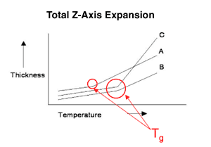 FIGURE 9: Expansion of three different base laminates. All post-Tg CTEs are higher than pre-Tg CTEs. Material A exhibits more total z-axis expansion than B because of a lower-Tg, but C, even with a higher Tg, exhibits more total z-axis expansion than A because it has a high post-Tg CTE.
 |
Perhaps even more important when selecting a Pb-free compatible material is the decomposition temperature, Td. Td is the temperature at which 5% of the mass of the material sample is lost to decomposition. Any mass lost during heating is not recovered. Even 2 to 3% loss, especially when exposed to multiple thermal cycles, can significantly degrade reliability. Materials with lower Td can decompose and become permanently altered during the reflow cycle. Figure 10 shows the decomposition curves for two different FR-4 materials with the same Tg – 175°C, as measured with thermogravimetric analysis (TGA).
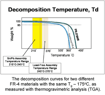 FIGURE 10: TGA of two laminate materials showing weight % loss during heating. FIGURE 10: TGA of two laminate materials showing weight % loss during heating. |
Soldermask may be a consideration during the Pb-free transition, as new flux and paste chemistries and higher processing temperatures may attack masks that perform well in the SnPb environment. Many brands and types of soldermask are available, check with the board supplier in advance. Also perform close visual inspection of the soldermask during the paste and flux evaluation cycles.
If peelable or temporary soldermask is used in wave soldering, it holds up with Pb-free fluxes and thermal excursions. Since the alloy has little effect on peelable mask, compatibility can be verified by running the current SnPb solder process with the anticipated Pb-free process parameters.
Some SMT adhesives are heat-reworkable. In other words, they are cured and hardened by heat (typically 125 to 150°C), but can be softened by applying more heat after the cure is complete. Because alloy metallurgy has little bearing on adhesive performance, adhesive compatibility can be checked in a method similar to that described for peelable solder mask.
Underfills should be tested for compatibility with new solder paste chemistries. Ideally, capillary underfill materials should demonstrate the same adhesion to Pb-free solder paste residues as with SnPb residues. This can be evaluated visually by cross sectioning, but thermal cycle and drop or vibration test data is preferable. No-flow underfills require more careful consideration. Because the cure rate of the underfill is matched to the reflow profile, the cure characteristics of the material will likely need to be changed by the material’s supplier.
Rework flux is usually the same flux used in the assembly process. If fluxes are changing, any defluxers used in test areas should be tested for compatibility with the new assembly process chemistries.
Step 3: Prepare to segregate. Cross-contamination of Pb-bearing and Pb-free solders in the assembly process can be a costly mistake, as it could render all assemblies suspected of cross contamination to the scrap pile. Segregation efforts should be diligent and highly visible. If possible, during the transition period, designate assembly lines as Pb-bearing or Pb-free ONLY. If this is not possible, separate setup kits should be stocked for each line. The setup kit should include squeegee blades, spatulas, dispenser nozzles, soldering iron tips, rework materials and any other components of the assembly process that offer potential for cross contamination. Each component of the kit should be individually labeled as Pb-bearing or Pb-free for identification purposes in case they do not get returned to the kit immediately during line changeover.
Solder pastes should be stored in separate locations (refrigerators or cabinets) to prevent operators from taking a wrong container by mistake. Solder bar and dross should also be stored separately and clearly labeled. Many solder manufacturers are taking steps to aid operators in recognizing the difference between the two products by changing colors, shapes or legends on containers. In early stages of transition, keep solder materials secure, giving only line leaders or supervisors access until the labor force becomes accustomed to the segregation systems.
Stencils bring an opportunity to cross-contaminate two alloys if they are shared between the two processes. Manual stencil cleaning does not remove all the particles from the apertures. Many automatic stencil cleaners leave some paste residue behind also. If an assembly is transitioning to a Pb-free process forever, the stencil can be thoroughly cleaned and inspected under magnification to ensure its cleanliness, then labeled and moved to a separate storage location designated for Pb-free. If an assembly will be transitioning with some runs in Pb-free and some in SnPb (e.g., during qualification runs), purchase a second stencil. This will eliminate the concern of cross contamination and bring the added benefit of having apertures optimized for Pb-free paste.5 Most stencil manufacturers can aid in the identification of Pb-free stencils by etching “Lead-Free Only” in the foil, and some offer different color frames to provide a visual cue.
Step 4: Effectively communicate the change before it happens. Train inspectors and rework operators before running Pb-free product. A contributing factor to yield loss during a Pb-free transition is false failures. Often, solder joints that do not need touch up are touched up anyway. Solder joints that are touched up are typically logged as a defect in the factory data collection system. Possible reasons operators touch up solder joints unnecessarily include:
- The operator is not properly trained in visual inspection of Pb-free joints.
- The operator doesn’t think it is a problem but diligently opts to err on the safe side, since they are responsible for final quality of the assembly.
- The operator confuses the characteristics of lead-bearing and Pb-free because they are being moved between assembly lines during the shift.
Pb-free surface-mount solder joints look different than SnPb solder joints. Their surface is generally duller, their wetting angle shallower and they can resemble what is referred to as a cold joint in SnPb processes.
Pb-free wave solder joints can also look different from their SnPb counterparts. Often, the surfaces appear rough and cracked; this is normal and usually depends on the cooling rate of the joint. The joints can resemble a SnPb disturbed joint for alloys with a pasty range. Even operators unfamiliar with disturbed joints can be tempted to touch them up, based solely on the different appearance.
To avoid unnecessary rework, train operators early, provide visual references in the work area, avoid moving operators from Pb-bearing to Pb-free lines during a shift and appoint an expert on each shift whom operators can ask whether the joint needs touch up. This expert can be an experienced solderer, a line supervisor or someone from the training department.
Training and education does not stop with rework operators and inspectors. Every person in the factory who judges solder joint quality and uses a soldering iron must be trained. This can include personnel in test, final assembly or warranty/repair areas. For CEMs, customers will also need training to avoid unnecessary questions and/or returns.
Visual indicators are critically important. Board labeling should be different; e.g., different color backgrounds for bar code labels or an extra label identifying the product as Pb-free. This will prevent mix-ups downstream. Examples of the labeling conventions should be posted throughout the factory. Photos of quality Pb-free solder joints should also be posted.
Once an assembly line is dedicated to Pb-free processing, it should have plenty of visual indicators. The phrase “Lead-free only” should be on all equipment and tools used on the line. Operators should be prevented from trading equipment or tools between lines whenever possible. Some materials suppliers provide stickers or labels to their customers assist them in the transition.
Line leaders or supervisors should be included in the formulation of a communication plan. They can best advise the most effective means of communication to the labor force. Prior to the launch of a Pb-free transition, all levels of operations supervision should be briefed on the communication plan prior to its rollout.
Step 5: Validate the process. The equipment is ready, the soldering chemistries have been selected and the factory floor has been prepared for the transition. The only thing left is to run the process and validate it. Unforeseen issues are bound to arise during the first few runs, so a few short “shakedown” runs are suggested to address them. An assembly with multiple types and surface finishes of components should be selected to run through the Pb-free process and undergo the appropriate scrutiny:
- Full visual inspection of solder joints, residues and wetting properties.
- Full visual inspection of the substrate for signs of blistering, measling, delamination or soldermask peeling.
- Full visual inspection of all components and connectors, with particular emphasis on the plastics.
- Inspection of through-hole connectors for solder balls (solder-side for wave solder or topside for intrusive reflow).
- Cleanliness analysis.
- Cross-sectional analysis of assembly.
- Joint integrity testing, when applicable.
- Any non-conforming defects or process indicators are recorded and resolved.
Some reworked joints should be included in the validation phase. At least one device on the assembly, including a BGA, should be reworked prior to validation review.
Process validation can take place internally, or be sent to an independent laboratory for objective review. The party reviewing the assembly should be notified which devices were subjected to rework cycles.
Step 6: Refine the process. Assuming the validation assembly passed all testing, the process is ready for production. But like any change in the fundamental structure of a process, a learning curve follows the initial implementation. Since Pb-free alloys behave differently, parameter settings optimized for Pb-bearing may be suboptimal Pb-free.
In SMT, rates of midchip solderballing, tombstoning, skewing, and random solderballing and pull back (e.g., when printing on mask for intrusive reflow) will be different with Pb-free alloys. Voiding properties will also change, as Pb-free pastes use different flux chemistries. Self-centering properties of Pb-free paste will not be as strong as their SnPb counterparts, so placement tolerances and end-of-line defects will require monitoring.
In wave soldering, the slower wetting of the Pb-free alloys can cause more skips and less hole fill. The different surface tension can cause more bridges and micro solderballs.
Essentially, the processes must be re-optimized as production volumes come up to a level where significant sample sizes can be obtained. Some process inputs that may require re-optimization include stencil aperture design, reflow profile style and placement pressure and accuracy in surface mount assembly. Flux loading, wave contact, peel-off mechanics and cooling methods may need to be revisited in wave soldering.
When seeking process refinements, start with research. A multitude of resources describe new tricks of the trade. Many organizations publish results of optimization procedures at conferences. Proceedings are usually available online to members. Local professional society meetings offer opportunities to share findings with other local assemblers in one-on-one exchanges or to learn from visiting experts. Bulletin board Websites can offer excellent exchanges of opinions and information free of charge. Spending an hour reading the postings of other engineers can answer a lot of questions and provide excellent guidelines when setting up DoEs. Specific questions can be asked of experts by posting them on the Website and viewing the responses.
Suppliers of materials and equipment should be a prime resource in providing guidelines to process optimization. Suppliers’ engineers support numerous Pb-free implementations in a variety of assembly areas, build their knowledge bases quickly and should be able to provide credible opinions on what works.
Conclusion
This will be the year that most assemblers begin building with Pb-free processes. A multitude of factors must be considered when planning the transition. This article lists factors deemed most important by engineers from material and equipment suppliers who have been working on the transition. It is a starting point for assemblers. Appendix A is a synopsis of the considerations in checklist form. Assemblers using the checklist as a planning tool can easily add considerations unique to their situation or delete those that do not apply to their process.
The most important thing for an assembler to keep in mind during the transition is that they do not have to embark on the process alone. Materials suppliers, equipment suppliers, professional organizations and Websites are great resources. Research the work that has already been done. The upfront time investment will bring considerable payoff when the implementation actually occurs. n
References
- RoHS Directive 2002/95/EC of the European Parliament and of the Council of 27, January 2003.
- D. Mendez and R. Clarke, “Statistical Model of Printed Wiring Board and Stencil Alignment Issues,” Surface Mount International Conference Proceedings, April 1997.
- Eagle-Eyed One, an independent engineering firm that characterizes stencil printer performance.
- C. Shea, V. Van Velthoven, R. Tripp and R.S. Pandher, “Reducing Variation in Outsourced SMT Manufacturing Through the Use of Intelligent Stencil Systems,” SMTA International Conference Proceedings, September 2003.
- R. Pandher and C. Shea, “Optimizing Stencil Design for Lead-Free Processing,” SMTA International Conference Proceedings, September 2004.
- J. Belmonte. et al, “Self-Centering of Offset Chip Components in a Pb-free Assembly,” IPC/Jedec International Lead-Free Conference on Electronic Components and Assemblies Proceedings, March 2004.
- E. Kelly, “An Assessment of the Impact of Lead-Free Assembly Processes on Base Material and PCB Reliability,” Apex Proceedings, February 2004.
Bruce Barton is regional applications engineer and Chrys Shea is manager, R&D applications engineering, at Cookson Electronics Assembly Materials (cooksonelectronics.com). Joe Belmonte is project manger, advanced process group, and Ken Kirby is applications engineer at Speedline Technologies (speedlinetech.com).


Press Releases
- Adam Ryder appointed as Managing Director of Incap UK
- Metal Etch Services Opens New Motor City Facility to Meet Growing Midwest Demand
- Yamaha surface-mount line powers the future of specialized production at Inter-Company in Netherlands
- Matric Group Becomes the First U.S. Manufacturer to Deploy Panasonic NPM-GH Dual Lane SMT Technology