

2005 Articles
Pb-Free PCB Finishes for ICT
New solders can mean new finishes. How to decide which is best.
Reliable in-circuit test (ICT) depends on good electrical contact between the fixture probe and the solder-coated via or pad. When a sharp probe strikes, solder will initially yield because the contact pressure of the probe is significantly higher than the yield strength of solder. As the solder yields, the probe breaks through any contaminants on the test pad surface, permitting good electrical contact to the uncontaminated solder beneath. The deeper the probe penetrates the solder, the better the contact will be.
In a Pb-free environment, the basic mechanism for making good contact with ICT is unchanged. In fact, the yield strength of Pb-free solders is not significantly different than their lead counterparts. PCB finishes are changing, however, which can indirectly affect probing reliability. Each finish has benefits and weaknesses, impacting ICT in different ways.
HASL. Hot-air solder leveling is the predominant Pb-based surface finish used today. The process involves immersing the board in a SnPb alloy. Excess solder is then removed using hot “air knives.” Most PCBs use HASL to protect the copper surface.
HASL is the cheapest finish available and is solderable through multiple process and storage cycles. However, the flatness or coplanarity is poor when compared to some Pb-free alternatives. For ICT, HASL provides automatic covering of test pads and vias with solder for good ICT probing performance.
HASL is mostly thought of as a lead finish, yet there are some promising Pb-free HASL alternatives emerging. The increased complexity of boards with finer pitches and flatness requirements has exposed many limitations with the HASL-type finish and many manufacturers are looking at alternatives for Pb-free.
Immersion silver. During the solder process the silver layer gets dissolved into the solder, making an alloy on the copper surface that provides a reliable solder joint, especially for BGA packages. The contrasting color makes it easy to inspect and it is also a drop-in replacement for HASL during soldering operations.
Concerns over migration effects of the plated silver itself led many manufacturers to further investigate this finish, but development of anti-migration agents added during PCB fabrication have gone a long way toward addressing this issue.
Immersion silver has not been shown to have any impact at ICT related to fixture contact.
ENIG. Electroless nickel immersion gold has been around for some time and also has no impact at ICT related to fixture contact. It offers excellent coplanarity, solderability and withstands multiple reflows. Its higher per-unit cost may limit widespread adoption as a Pb-free alternative.
OSP. Using bare copper with organic solderability protection is gaining popularity due to cost benefits of not having any additional metal finish on traces other than a thin organic preservative. Unlike other PCB finishes, it leaves no solder on the testpads or vias. This is a problem for ICT probing, since raw copper has yield strength an order of magnitude higher than solder. A sharp probe cannot penetrate the oxides that build up soon after the OSP compounds boil off in the reflow oven, resulting in poor contact at ICT.
Some manufacturers have used higher force probes and multiple fixture actuations to work around this problem, with limited success (Figure 1). Therefore, SMTA guidelines recommend never probing raw copper OSP. Instead, the stencil should be opened to paste testpads and vias. This will provide a soft solder-coated surface for good contact after the board is reflowed.
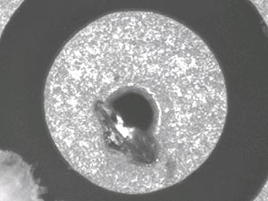 FIGURE 1: A raw copper via damaged after being hit with a 3N “dagger” test probe 12 times.
 |
Once solder is applied to test points, parameters like flux content, paste volume and test limits may still need to be adjusted.
The move to Pb-free presents a challenge for ICT since PCB finishes will likely change. Some recommendations:
- Ensure that test engineering is involved in Pb-free discussions and trials. Do not just focus on the process.
- Explore all aspects of Pb-free finish alternatives, not just the unit cost saving for OSP finishes, for example.
- If you choose OSP, be sure to apply solder paste to the test pads and vias – all testability guidelines recommend this.
Stig Oresjo is a senior test strategy consultant with Agilent Technologies (agilent.com); 970-679-3215. Chris Jacobsen is technical marketing specialist, manufacturing test business unit.


Press Releases
- Green Circuits Announces Strategic Partnership with Metatron Private Equity
- Smartsol Technologies Mexico Strengthens its X-ray Division and Announces Strategic Partnership Expansion with Creative Electron
- Hanwha Semitech Americas Supports Regal Technology Partners with New SMT Line Installation
- AIM Hires Marcus Pee as Sales Engineer for Southeast Asia