Yardsticks for Gauging AOI Effectiveness
A 95% first-pass yield is the litmus test. Here’s how to get there.
Capital spending is an internal issue EMS providers constantly grapple with. At the back of the minds of the decision-makers are a host of related and nagging questions. Can we make do with existing equipment?
What are our tradeoffs? Will we lose money using older assembly equipment? How will customers perceive older equipment? Can we satisfactorily deliver to OEMs with cutting-edge technologies?
Of all the associated capex questions, the most prominent should be: Do we provide the right levels of technology, manufacturing equipment and expertise to deliver the best product to the OEM?
One way to get there is through sophisticated automated optical inspection systems. The extraordinarily small component packaging and ever-shrinking PCB sizes require superior inspection solutions to detect assembly flaws and defects.
AOI is well-suited for checking tombstones, misaligned or missing components, wrong polarity, wrong parts, lifted leads, and lifted lead banks. AOI ensures that installed components are the right ones in terms of value and footprint. It also catches marginal opens, in which the assembled joint is minimal and certainly not 100%. In many cases, when the AOI operator manually presses on the joint in question, the connection is made.
When older AOI technology is used on the assembly floor, it often is in conjunction with testing, and the latter is expected to catch those latent defects that slip past AOI. A better process, however, is to upgrade the AOI machines. New features include advanced LED lighting, the color of that lighting, camera location, lens resolution, user interface, and better, more comprehensive algorithms for detecting components and flaws.
Beyond the equipment itself, the AOI operator or programmer plays an equally important role. AOI is designed to detect questionable components. However, it’s up to the operator to ensure defects are either “true” or “false.” One aspect they must be mindful of is defining the tolerance or pass code as tightly as possible for defining the right window for reading components on a PCB. Within this tweaking process, if the tolerance window is too tight, it can be increased. But if the region of interest is made too big, then the AOI passes virtually everything, and true faults will be missed.
The experienced AOI programmer will program the right part type, and accurately program the tolerance or pass code. In this second step, the operator performs program tweaking to train the AOI for the right component, as well as define the tolerances, the footprint, size of the rectangle, and the overall region of interest.
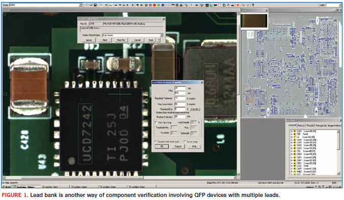
Figure 1 shows the lead bank indication on the AOI monitor. It is yet another way of component verification involving QFPs that have multiple leads. In this case, highly complex algorithms are put to use to inspect these particular components. These lead bank windows are larger in size to not only perform component verification, but also expedite the inspection process.

Compared to the earlier incandescent AOI lighting systems, LED technology has provided AOI operators superior brightness and a clearer, sharper focus on devices and hard-to-see board areas. Also, LED lighting spreads out the viewing area more uniformly to track down flaws and defects in the subject target or “region of interest.” Another advantage LEDs offer is the availability of different colors.
The color white is traditional. But LEDs allow the application of different color filters such as blue, red or an RGB (red, green, blue) option. These filters are especially valuable to improve visibility on small or overly shiny components.
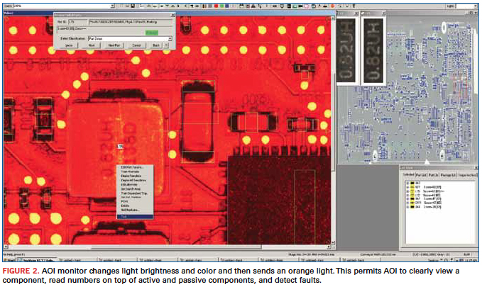
For example, a traditional white light immediately reflects off a glass-based package in the region of interest, creates a blank, and prevents the viewing of that component. Using advanced AOI features, the operator applies the different filters during programming or simply applies the different color lighting if already programmed. Figure 2 illustrates such a case where AOI changes light brightness and color and then sends an orange light. This permits the AOI to clearly view a component, read numbers on top of active and passive components, and detect faults.

As for camera locations, an effective AOI has five different viewing sites. One is on the left, another on the right, the third on the front, another on the back and one on top. This way, a board is captured from every angle. If component markings cannot be viewed from the top, the operator has the option of going to the side angle for a different view and the ability to detect that component. Having different cameras at different locations is a great help in determining and detecting true failures compared to false failures. A greater number of cameras offer better visibility on different sides and different angles with greater depth of field, giving greater coverage of the region of interest. Consequently, true and false faults are clearly seen with no visual ambiguities.
Newer AOI technologies have also introduced higher camera lens resolution. Today’s state-of-the-art AOI cameras sport 25MP. Five years ago, AOI featured 1MP cameras. The big jump in megapixels is providing considerable capability for component feature recognition and a much clearer view. These extra megapixels hand the operator a highly consistent and crisp picture of extremely small areas on top of components. These viewing advances come at a time when such passives as 0402, 0201 and now 01005 are so small that the human eye can barely see them. But with this large number of pixels, they can be clearly spotted.
Two other complementary features are zoom capability and depth of field. Particularly for extraordinarily small component packaging and tight PCB areas, the newer cameras can zoom in from 50 to 250X to closely view those shrinking board areas. Meanwhile, depth of field spreads out the region of interest and makes it considerably sharper to clearly view and locate any possible flaws.
User Interface and Algorithms
The effectiveness of an AOI user interface and the comprehensiveness of its supporting algorithms are synonymous. Operators and technicians solely depend on their AOI’s visual images of the good and bad components or the true or false nature of the devices under inspection. Generally, those are the most effective AOIs today since those are the ones that catch considerably more true versus false faults.
In particular, considerable concentration and effort go into developing and writing the supporting AOI algorithms. In effect, the way this software is written determines how well – percentage-wise – images can be seen and located. The quality of the algorithm can determine whether suspect images are caught by a few percentage points or by a big number. This also means the comprehensiveness of these algorithms must capture images, not only the black and white, but also all the shades of gray in-between or those faults in a “maybe” category.
Those gray areas are becoming more troublesome these days due to shrinking PCB sizes and component packaging, which have generally shrunk 30 to 40% and maybe even more in the past five years. That means smaller packages have a smaller space on which to write with extremely fine type nomenclatures and numbers or the component manufacturer’s name and logo.
Also, it’s important to note that some components today are laser-marked on the sides. In cases like these, a robust algorithm is able to not only shine the light on the side of the component, but also to accurately determine the nomenclatures or numbering laser-etched on the side. Sometimes these laser etchings may not be completely visible with a regular AOI camera. But advanced AOI can certainly capture these faults.
Results obtained through AOI show the levels of first-pass yields achieved. State-of-the-art AOI can detect 99.5% of component faults and failures. Older AOI technology, on the other hand, detects perhaps 80 to 85% of the defects. The question, then, for the assembler, is: What is the value of this additional 12 to 15% detection rate that seriously affects first-pass yields?
A 95% or higher first-pass yield provides the litmus test. OEMs of some end-products demand considerable quality and reliability from the outset. Others might get by with older technology. If defects and flaws aren’t caught at the AOI stage, the PCBs carrying those problems undergo visual inspection or functional test. PCBs aren’t 100% testable. Thus, it’s possible a bad component might slip through AOI and go undetected to the field, especially if the module with the bad component doesn’t undergo testing. Advanced AOI largely eliminates inconsistent visual inspection and reduces dependency on functional testing to ensure defects and flaws are caught early on.
Zulki Khan is president and founder of NexLogic Technologies; zulki@nexlogic.com.
Press Releases
- Distron Corporation Expands In-House Capabilities with Automated Conformal Coating for Complex PCB Assemblies
- Eastek International Corporation Appoints David Strabel as Vice President of Manufacturing
- SEMI Projects Double-Digit Growth in Global 300mm Fab Equipment Spending for 2026 and 2027
- Koh Young Announces Two Sales and Service Changes to Strengthen its Customers in the US and Canada


