

Advances in Fine-Pitch Printing Process Technology
Achieving sufficient paste volume fill of fine-feature apertures is tied to stencil design.
The challenges of fine-pitch printing have inspired some creative thinking in manufacturing engineers, and it’s also fair game to explore the possibility of modifying existing materials to achieve acceptable results. After all, obtaining high yields achieves nothing in the end if the cost of doing so negates profitability. In fact, we maintain that under most conditions, electroformed and nanocoated stencils aren’t necessary at all, but rather a different way of thinking about stencil apertures and how to optimize their design to achieve best results with fine-pitch, given a few “rules” about the basics of area ratio and how it affects solder paste printing, no matter the stencil material or type of printer used.
We maintain that it possible to achieve better yields using a standard laser-cut stencil, but that rethinking and modifying (or “editing,” as the major stencil houses like to say) the Gerber data for the stencil aperture cut can produce better results with fine-pitch.
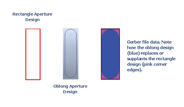
Figure 1. Rounded-off corners on rectangular aperture designs facilitate paste release for fine-pitch designs.
Fine-pitch printing results are directly tied to stencil aperture area ratio, a relationship between aperture area and stencil thickness. One may not be able to control the size of the fine-pitch pads that the stencil is being fabricated to print onto, but printing results can be enhanced by modification of aperture design, keeping a few principles in mind.
(It might also be suggested that building and maintaining a good working relationship with one’s stencil house is invaluable, not only when creating the stencil design and patterns, but at every step in the stencil’s fabrication process, so that a thorough understanding of the possibilities (as well as limitations) is shared and well understood. The knowledgeable counsel of experienced stencil fabricators can help prevent many print and downstream defects and issues that might be prevented at the design stage.)
When designing aperture cuts, keep the principles of area ratio in mind. For example, when calculating area ratio, which incidentally is 0.66 for laser-cut stencils, best results are obtained when aiming for the happy median of that number. A number too far to the left (or right) of 0.66, for example, could result in defects in downstream manufacturing.
The appropriate stencil thickness ensures proper paste release from the stencil. The aspect ratio for rectangular apertures should be 1.5, and the area ratio 0.66. It is best to evaluate the smallest apertures on the stencil to determine the proper stencil thickness.
The following formulas are used to select an appropriate stencil thickness:
- Aspect ratio = Aperture width (W) / stencil thickness (T) [should be 1.5]
- Area ratio = Area of pad (L x W) / area of aperture walls (2 x (L x W) x T) [should be 0.66]
It is more common to use area ratio as a guide to paste-transfer efficiency. Area ratio is the area beneath the stencil aperture opening, divided by the area of the inside aperture wall. For a rectangular aperture, the area ratio = [(L×W)/2(L+W)T)], where L and W are the aperture length and width, respectively, and T is stencil thickness. For a square aperture, area ratio = S/4T, where S is the side of the square. For a circular aperture, area ratio = D/4T, where D is the diameter of the circle.
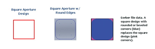
Figure 2. Rounded corners on square aperture designs.
The generally accepted rule is to achieve area ratios of >0.66 for paste transfer. The advent of electroformed stencils has made it common to print apertures with area ratios down to 0.50.1
The definition of aperture area ratio is the area of the stencil aperture opening divided by the area of the aperture side walls. A simple calculation shows that area ratio (AR) reduces to diameter (D) of a circle divided by four times stencil thickness (t): AR = D/4t. It should be noted that results for circular apertures are the same values as are calculated for square apertures, with D now equal to the side of the square (formula for calculating area ratio).
Here are some stencil aperture design recommendations the author has found work well as a process engineer:
Rule 1: Round the corners. A square SMT pad doesn’t require a square aperture. The key is volume of paste deposited, which should be consistent every time. Solder paste tends to remain in sharp corners of square apertures, not depositing on the pad as it should and thereby causing clogs. This results in print defects (insufficiencies or missing), and if not detected, soldering defects such as starved solder joints (or no solder joints). The high surface of the inside of the aperture at the corners, versus the pad surface area, will cause paste to adhere to the aperture walls in those corners and not transfer to the pad after a print stroke. Instead of using a rectangle aperture cut design, use an oblong aperture cut. Getting rid of the sharp corner edges will reduce the potential of paste clogging in the corners. Wetting out to the corners of the pad during reflow should not be a problem with good solderability (pad) and an optimized reflow process, lead-free notwithstanding.
Rule 2: BGA pads – the beveled rectangle. The opposite principle actually applies to a BGA pad, which is, understandably, circular. However if the circular pad (and aperture) are very small in diameter, the shape itself can negatively affect print registration, especially for very fine-pitch packages of chip-scale size and µBGAs. The emergence of compact smartphones and mobile/wireless devices is driving expanded use of 0.3mm ultra-fine-pitch µCSPs, µBGAs and other active devices. For example, for a two-layer CSP, 0.3mm pitch means that the distance is 11.8 mils between the center of a given solder ball and the center of the next solder ball. Added to that, under older design guidelines, a solder ball joint pad would be designed with the diameter of 20% less than the diameter of a BGA/CSP solder ball; i.e., using the formula A = B = 80% x ball-diameter, where the size of the aperture is actually 80% of the diameter of the pad size.2 So we’re dealing with very tiny apertures and for fine-pitch or µBGAs. The author’s experience has shown the best results are obtained by turning the circle into more of a square with rounded or beveled edges – a beveled rectangle, if you will. This will produce better print registration yields. The squaring of the shape (FIGURE 3) is not enough to cause bridging, even if it falls slightly outside of the land area. Stencil foils of 125 to 150µm thickness are standard for this application, but to maximize yields, good release, consistent solder paste volume and optimized aperture shapes are critical, especially as ball pitches decrease.
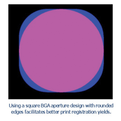
Figure 3. Reverse strategy for BGA apertures, i.e., squaring the circle slightly.
Experimental Results
A stencil for printing fine-pitch SMT pads was created using the abovementioned guidelines for aperture design. Print tests were run and the results recorded, using data obtained from a solder paste inspection (SPI) machine. The histograms for each component footprint (FIGURES 4 to 13) basically compare the average (mean) volume percentage, area percentage and standard deviation.
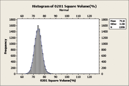
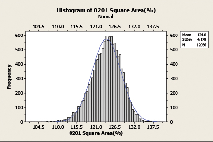
Figure 4. 0201 square aperture. Pad size: 0.012" x 0.018". Area ratio: 0.9.
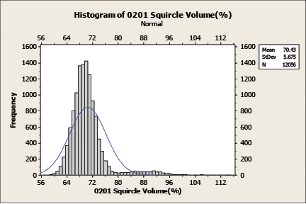
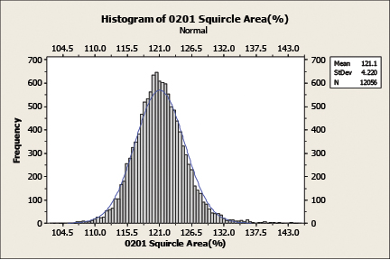
Figure 5. 0201 square with rounded corners. The goal with rounded corners is to reduce volume to avoid tombstone defects and eliminate the possibility of clogged apertures. Pad size: 0.012" x 0.018". Area ratio: 0.9.
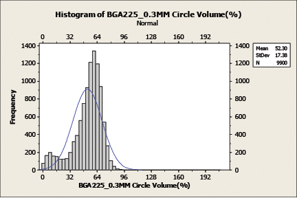
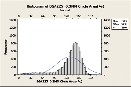
Figure 6. BGA 225, 0.3mm pitch with circle apertures. Pad size: 0.006" diameter. Area ratio: 0.375.
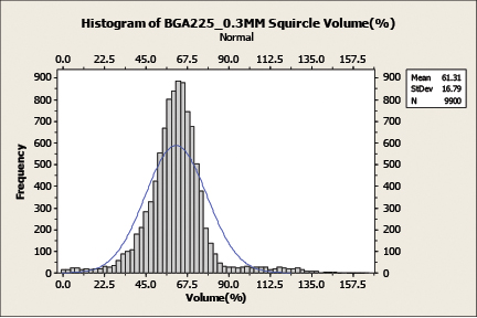
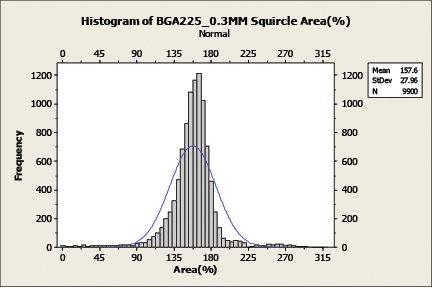
Figure 7. BGA 225, 0.3mm pitch with square/rounded corner apertures. Volume is a little higher, but the process is more
repeatable to hit the average (mean). Pad size: 0.006" sq. Area ratio: 0.375.
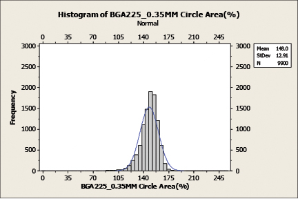
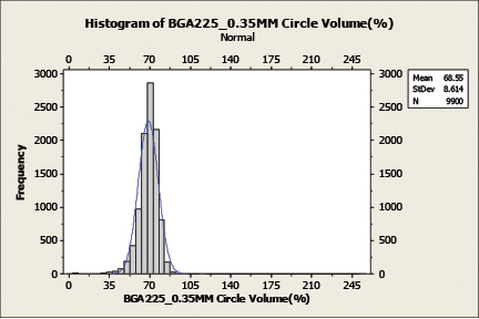
Figure 8. BGA 225, 0.35mm pitch with circle apertures. Pad size: 0.007" dia. Area ratio: 0.4375.
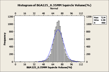
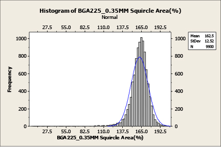
Figure 9. BGA 225, 0.35mm pitch with square/rounded corner apertures. Higher volume % due to better print registration with “squircle” apertures. Pad size: 0.007" sq. Area ratio: 0.4375.
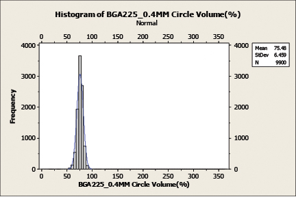
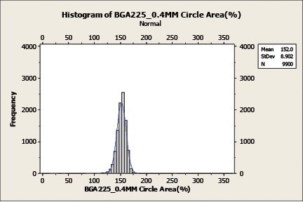
Figure 10. BGA 225, 0.40mm pitch with circle apertures. Pad size: 0.008" diameter. Area ratio: 0.5.
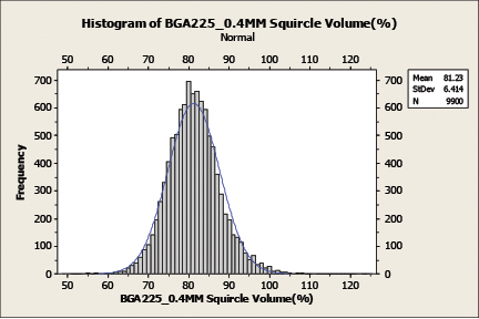
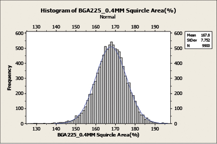
Figure 11. BGA 225, 0.40mm pitch with square/rounded corners apertures: Higher average volume % and better standard
deviation = more repeatable prints. Pad size: 0.008" sq. Area ratio: 0.5.
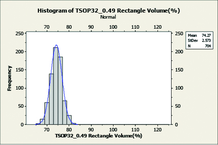
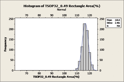
Figure 12. TSOP 32, 0.5mm pitch with rectangle apertures. Pad size: 0.060" x 0.012". Area ratio: 1.25.
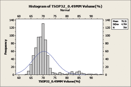
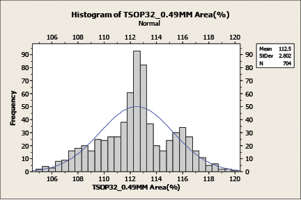
Figure 13. TSOP 32, 0.5mm pitch with oblong apertures: The goal with oblong apertures is to reduce the potential for shorts; hence the smaller average volume and area coverage. Pad size: 0.060" x 0.012". Area ratio: 1.25.
Process program parameters:
- Board size: 10" x 8"
- Force: 19 lb.
- Speed: 1.5"/sec.
- Squeegee blades: 12"
- Solder paste: Indium 3.2 (Pb-free) Type 4
- Separation profile: N/A
- Wiper profile: Vacuum, solvent and dry wipe after each print
- Stencil thickness: 4 mil (laser-cut)
Conclusion
In almost every example, following the aforementioned stencil aperture design guidelines the edited stencil apertures exhibited higher print volume and area percentages, and also exhibited a lower standard deviation, which indicates the modified stencil is more repeatable in terms of results (good volume percentage) for these fine-pitch printing applications.
References
1. William E. Coleman, Ph.D., and Michael R. Burgess, “Choosing a Stencil,” SMT, July 2006.
2. Michael Yu, “Taking on the 0.3mm Ultra-Fine-pitch Device Challenge in PCB Design,” Embedded, October 2011.
Ed.: This paper was first presented at SMTA International in September 2014 and is reprinted with the author’s permission.
is senior printing application sales engineer at Speedline Technologies (speedlinetech.com); ismith@speedlinetech.com.


Press Releases
- Seika Machinery’s SMI 2026 Webinar Series Continues with Focus on PCB Cleaning Before Solder Paste Printing
- Forwessun Expands Testing Capabilities through Strategic TRI Alliance
- Federal Electronics Expands Advanced Manufacturing Capabilities to Support Military and Aerospace Cable Assembly and Wire Harness Programs
- Altus Continues Irish Growth with Expansion of Engineering Team