

X-Ray Imaging of Pb-Free Solder Joints
The ability of x-ray inspection to nondestructively inspect components for various imperfections such as cracks and voids serves as an ongoing quality control methodology to assess materials and optimize assembly processes. Existing x-ray systems can be used for inspecting Pb-free assemblies without modification. However, because of the density variation between tin, copper and silver predominant in Pb-free alloys, it is recommended that certain x-ray tube parameters be adjusted when inspecting Pb-free BGA and chip-scale package devices to ensure optimal image contrast and enhanced analysis.
Understanding these material density variations helps explain the role that adjusting and optimizing x-ray tube parameters and test routines plays in providing a vital and sound method of investigating all aspects of device and PCB processing with respect to identifying defects in a production environment.
Any object or material within an analyzed sample that has a higher density than its surroundings will absorb more of the x-rays in that specific location. As a result, fewer x-rays will pass through the sample at that location, resulting in less x-rays hitting the capture device at that point, thus casting a darker shadow on the detector. A typical x-ray image produced by an x-ray inspection system has solder locations, device terminations and copper tracks appearing darker compared with the laminated circuit board or substrate material. The greater the density difference between the materials in question, the more clearly the contrast will appear on the x-ray image.1
The quality of the x-ray radiation produced by an x-ray tube, and its effectiveness in discriminating the different materials within a sample to produce a useful analytical image, depends on the particular x-ray tube settings used. These settings are referred to as the x-ray tube accelerating voltage, or kilo volts (kV), and the tube power, or watts (W) used to set the tube at appropriate levels to obtain an image with optimal contrast at the detector.
The accelerating potential is the applied voltage between the anode and cathode of the x-ray tube. Electrons are produced at the cathode and accelerated striking the target anode creating x-rays. The tube power is calculated from the product of the accelerating potential and the electron current hitting the target, which is usually made of tungsten. The more power used, the brighter the x-ray source; however, there are technical limitations on the maximum power that tubes can achieve.
The kV setting is also a measure of the penetrating power of the x-rays. The higher the kV used, the more penetrating are the resulting x-rays. This means higher kV levels need to be used to image dense or thicker objects. Conversely, at lower kV levels only thin or less dense samples are inspected.
The interaction between penetrating radiation and matter, such as x-rays passing through a sample under test, is a complex relationship based on a number of factors. An important consideration is that absorption of the radiation increases with the atomic number and density of the material that is present.
Material Properties
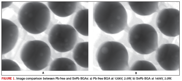
Historically, the most common SnPb solders have consisted of 63% tin and 37% lead. The most prevalent Pb-free solder alloy in use today is the SAC alloy, which contains a mixture of tin, silver and copper. Although different alloys available from various suppliers have varying elemental ratios, the majority of SAC alloys contain approximately 97% tin.
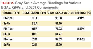
Table 1 shows the differences in the atomic number (Z) and density between the different elements contained in SnPb and Pb-free solders. Lead has a very high Z value and has been replaced in Pb-free solder alloys with an increased quantity of tin, which has a much lower Z value, as well as a lower density. Therefore, the effect of imaging Pb-free solders using the same x-ray tube parameters used for SnPb solders may result in the image being overexposed. This is because the lower Z value and less dense materials contained in Pb-free alloys will absorb fewer x-rays, permitting more to pass through to the detector, potentially saturating it.
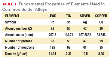
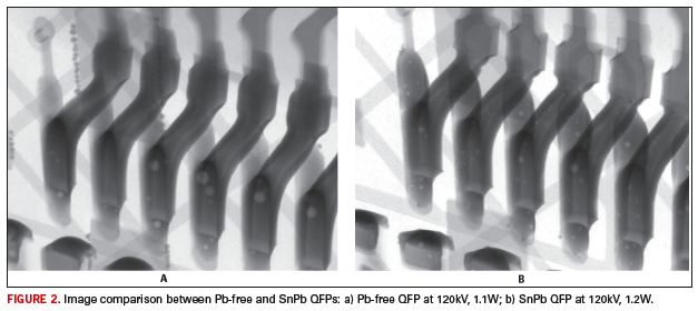
This difference in Z value and density between Pb-free and SnPb solders can be noticeably observed when imaging the solder joints for a variety of components with different mass and thickness (Table 2). The measurement data consist of average gray-scale readings obtained from 30 readings of each type of component with background variations accounted for, as well as the calculated differences between Pb-free and SnPb images.2 The x-ray parameters kV and power level were kept the same for Pb-free and SnPb components for these readings.
To compensate for this effect, it is generally necessary to decrease the tube kV and/or the power values that have been used for x-ray inspection of SnPb solder when inspecting assemblies produced with Pb-free alloys. This will ensure suitably contrasted images are available for analysis. However, these changes are very small in quantity with decreased values of 5-20 kV for accelerating voltage and/or 0.1-0.25 for power. This also depends on the x-ray system being used, due to variations in tube efficiency, capability and brightness from manufacturer to manufacturer.
Optimizing X-Ray Parameters
When optimizing x-ray tube parameters, the actual adjustments are to a great extent dependent on the thickness and mass of the solder joint for various components. In the case of BGA components, it is suggested to lower the kV value when inspecting a Pb-free solder joint (Figure 1).
For Pb-free components that have thinner solder joints, such as a quad flat package or an 0201 discrete component, a slight lowering of the power setting and/or the kV will achieve an optimal image (Figure 2 and Figure 3).
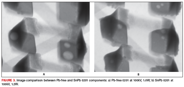
As can be observed from the figures, adjusting the x-ray tube parameters with a lower kV or power level optimizes the image quality of Pb-free solder joints and facilitates a complete analysis of potential defects such as cracks or voids, as well as other manufacturing anomalies.
The key requirement of x-ray inspection is that hidden defects such as cracks, opens, bridges, shorts, voids, etc. can be seen so that process and quality control can be maintained throughout the assembly process. Inspecting Pb-free solder joints requires consideration be given to the implications of the material differences exhibited by the elements present to ensure that optimal image quality is maintained to enhance manufacturing process yields.
References
1. David Bernard, “An A-to-Z Guide to X-Ray Inspection,” Circuits Assembly, December 2007.
2. Evstatin Krastev, “X-Ray Image Comparison, Lead-Free and Tin-Lead Boards,” IPC/JEDEC Lead-Free Reliability Conference, December 2007.
Dr. Evstatin Krastev is applications manager for semiconductor packaging and printed circuit board inspection at Dage Precision Industries, a Nordson Co. (dage-group.com); ekrastev@dage-group.com.


Press Releases
- Javad EMS Upgrades Through-Hole Soldering Capacity with New SEHO PowerWave System
- Sharpen Your Selective Soldering Skills with Kurtz Ersa's July VERSAFLOW 4/55 Training
- Omron Advances Inspection Technology with NVIDIA Omniverse and Metropolis
- Seika Machinery’s SMI 2026 Webinar Series Continues with Focus on PCB Cleaning Before Solder Paste Printing