

From the Archives: Design and Assembly of 01005 Passives Using Pb-Free Solder
This study finds a process similar to 0201 parts, with a 100 µm thick stencil and a nitrogen environment.
The use of 01005 size passives poses a number of challenges. First, a feasible screen-printing process must be achieved. To achieve a high-yield soldering process, a sufficient amount of paste is needed and variations in paste volume must be minimized. Many factors influence screen-printing quality: stencil thickness, paste characteristics, paste type (particle size) and printing parameters such as printing speed, pressure and separation speed. Other factors such as the mechanical condition of the stencil, cleaning frequency, flatness of the circuit board and the method of supporting the PCB during screen printing also contribute to the process capability.
The next question concerns pick-and-place. The capability of current equipment for accurate, repeatable alignment must be verified, as does the ability to physically handle these extremely small parts. The placement accuracy required depends on the ability of the components to self-align during reflow. Theoretically, self-alignment is determined by solder paste composition (eutectic SnPb versus lead-free), reflow atmosphere (which may change the surface tension of the solder), and surface finish.
Our first objective was to establish a land pattern design that permits a high assembly process yield and maximizes real estate saved. The second task was to evaluate and develop screen-printing and pick-and-place processes for 01005 components (Figure 1).
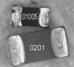 |
| FIGURE 1. Comparison of 0201 and 01005 components. |
An array of land patterns (Figure 2) for 01005s was designed and incorporated on a test vehicle (Figure 3) that was already being laid out. The TV was 170 x 145 x 1 mm, but the test structure for an array of 816 component sites for 01005s only used a small portion of the TV. The TV was 1 mm thick, had six copper layers and FR-4 laminate core material.
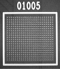 |
| FIGURE 2. The 01005 test sites. |
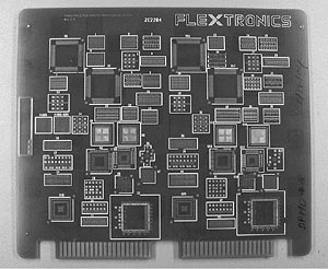 |
| FIGURE 3. Test vehicle. |
The components used were resistor and capacitor dummy parts provided by two different suppliers. The size of the capacitors was found to be within specified limits. The typical size is 0.39 x 0.19 mm with a termination width of 0.08 mm. As a general comment, the parts were well-defined and seemed to have only small, acceptable variations. Even though too few parts were measured to statistically support this statement, the reasonable reject level from the placement machine offers some additional credibility. There were, however, some irregularities of the component termination edge where it meets the ceramic body, possibly nozzle imprints caused by the taping equipment.
The 01005 components are supplied in regular 8 mm tape with 2 mm pitch between the pockets. During these trials, the carrier tape did not appear to cause any particular problems, even though component pocket tolerances should be critical. For 01005s, a relatively large gap between the component body and the tape pocket exists, as compared with what is usually seen with 0201s.
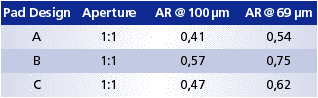
Pad design optimization. In the first experiment, two different pad designs were tested. Most were paste printed, but some 01005 dummy resistors were placed on double-sided tape. After this initial trial, the results were analyzed and another pad layout was designed based on those results. Changes made to the design were based on the collected solder paste printing data for the corresponding aperture, pre- and post-reflow inspection, including visual inspection using light microscope, x-ray and SEM, and shear testing of the soldered parts. The difference between the three different pad designs is relatively small, but still critical to successfully processing these miniature parts. Factors such as component size and tolerance, PCB manufacturability, placement accuracy, process variations and product reliability must all be taken into consideration.
In the initial trial, SnPb solder was used on an ENIG (electroless nickel immersion gold) finish. In the second experiment, lead-free solder was used on an OSP (organic solderability preservative) finish. A 100 µm thick stencil was used.
As in Figure 4, pad design A used in the initial trial was found to be too small in both the x and y directions. No pad surface is available to permit proper wetting, and the pad width is smaller than the component width. This mismatch can be attributed to the fact that the tolerances of the 01005 parts were not fully known at the time the pad was designed. The first set of experiments also showed that it was not possible to achieve acceptable paste printing results with this layout.
 |
| FIGURE 4. Pad design A. |
The other pad layout (pad design B) from the first set of experiments appeared more promising. In this case, the pad width is sufficient and there is clearly enough room for a wetting angle to form. With this layout, visual inspection of the printing result also looks acceptable, even though an acceptable process capability for the print volume was difficult to achieve and maintain. Figure 5 shows a dummy resistor mounted on double-sided tape using pad design B.
 |
| FIGURE 5. Pad design B. |
Since a main reason to use these parts is the size reduction, it is important to minimize pad size without sacrificing yield. Based on the results, it appeared possible to further optimize the design so a third pad layout, with dimensions in between the previous two, was designed. This design (pad design C, Figure 6) was chosen for the continuing experiments.
 |
| FIGURE 6. Pad design C. |
The second iteration layout was used in another trial where approximately 1,600 dummy capacitors were placed on lead-free solder paste and reflowed. In this trial, the component sites were laid out with 150 µm pad-to-pad spacing with no soldermask between the soldering surfaces.
Stencil aperture. The target was a 100 µm thick, laser-cut and electropolished stainless steel stencil, which is considered as a low-cost option for volume manufacturing. Previous experience and earlier studies have shown that electroformed stencils and stencils with a lower thickness could potentially outperform the described stencil. However, in actual applications, thinner stencils may not be able to provide sufficient solder paste volume for the other components on the board, and electroformed stencils generally cost more than laser-cut stencils.
Based on Flextronics’ previous experience with 0201 and other miniaturized pads and apertures, the optimal solder amount was calculated and transformed into a stencil aperture. Three different stencil aperture sizes were investigated, one for each pad size (Table 1). The area ratios (AR), defined as the ratio of the opening area of the aperture to the wall area of the aperture, were calculated and considered.
 |
| TABLE 1. Area ratio comparison. |
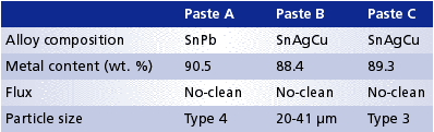
In the first experiment, a type 4 solder paste with eutectic SnPb composition was used. For the second experiment, two different lead-free solder pastes were initially compared for 01005 printing. These had previously been evaluated and selected from a larger number of pastes. A summary of the solder paste properties is provided in Table 2. After an initial printing trial, where printing parameters were also optimized, one of the two pastes was chosen based on volumetric measurements and process capability calculations. The chosen solder paste had a no-clean flux (L0), Sn3.9Ag0.6Cu alloy and a particle size of 20-41 µm.
 |
| TABLE 2. Solder paste properties. |
The objective was to establish a viable paste printing process for 01005 components. The criterion for a successful paste printing process was achieving a Cp value of 1.33 with an upper tolerance limit of +50% and a lower tolerance limit of -50% of the average measured volume with no bridges formed between paste deposits.
A regular screen printer with metal squeegees at 60° was used. Good board support could be achieved using an array of support pins. The printer was set up with automatic dry wipe between every board, and printer settings were optimized through DoE (design of experiments) based on volumetric print measurement results. The printing pressure was set at 12 kg, printing speed at 40 mm/sec. and separation speed at 10 mm/sec.
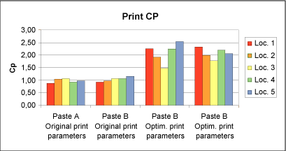
The separation speed was found to have a strong influence on the printing result. The difference between the two pastes is very small, while the improvement after optimization is large (Figure 7). The printing quality was also verified with visual inspection under microscope. Some flux was observed bleeding out from the deposits (Figure 8), which overall looked well-defined and uniform.
 |
| FIGURE 7. Optimization of printing parameters. |
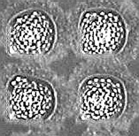 |
| FIGURE 8. Solder paste deposits. |
One main interest was to see whether the particle size of the paste would make a significant difference. No missing solder, judged as fewer than five solder particles on a pad, was found in these samples. As can be seen in Figure 7, both the lead-free pastes exceeded the minimum Cp requirement of 1.33 after optimization. A finer particle size provides a better paste release and a slightly higher Cp value; however, it can be more expensive and may be more prone to solder balling. In this work, paste B was used for further investigation.
For each aperture, more than 1,600 deposits were inspected. No missing paste was found on these samples. Even though three setup boards were printed before the measured prints, a clear improvement can be noticed over the four boards printed for the 01005 assembly (Figure 9).
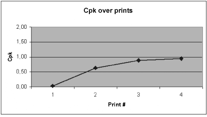 |
| FIGURE 9. Cpk value improvement after three setup prints. |
GR&R. To facilitate the analysis of the paste printing process for 01005s, an automatic 3-D solder paste inspection system was used to measure the volume of each printed deposit. First, a GR&R (gauge repeatability and reproducibility) study was conducted. As the true process variation for 01005 was not known, a tolerance of ±50% was used for the calculation. Appraiser variation is typically negligible when an automatic system is used, so this parameter was not used.
The GR&R was calculated to be 15%, which was judged acceptable at this point. The GR&R calculated for 0201 size deposits was 9%. To verify further that the measurement accuracy was sufficient, the data collected for the GR&R was plotted graphically. Figure 10 shows that the measurement variation is much smaller than the process variation, as each line represents one measurement run, and each location is repeatedly measured with almost the same result.
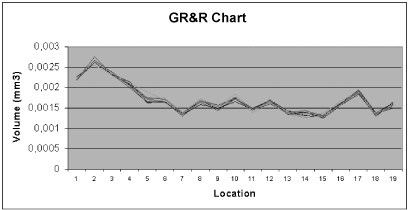 |
| FIGURE 10. GR&R data. |
Component placement. Placement was performed using a pick-and-place machine with a revolver head. The machine was previously upgraded for 0201 placement and had a high-resolution camera; no modifications were made to the machine apart from adding suitable 01005 nozzles. An array of support pins was used to stabilize the boards during assembly.
To determine the accuracy required for pick-and-place equipment to place 01005 components, the self-alignment of misplaced components during reflow was studied with 01005 components reflowed on SnAgCu paste in nitrogen atmosphere. A slight misplacement (45 µm) of selected components was measured after placement (Figure 11), but these parts were found to be well-aligned after reflow (Figure 12). Therefore, up to 45 µm misalignment can be accepted in pick-and-place process, under the experimental conditions.
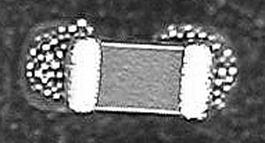 |
| FIGURE 11. 01005 dummy capacitors misaligned by 45 µm in pick-and-place process using SnAgCu solder paste. |
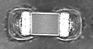 |
| FIGURE 12. The component has fully aligned after reflow. |
In this second trial 1,600 placements were made. Vision recognition rejects were collected from the machine and found to be 2.4%. All parts were visually inspected under microscope after placement, and no defects were observed. Based on the assembly results, it appears that pad design C, which is smaller than the B version, still offered a target large enough for successful placement to be achieved.
Reflow soldering. Reflow was carried out in a reflow oven typically used for high-volume manufacturing with eight heating zones and one cooling zone. The lead-free temperature profile used for the SnAgCu solder is shown in Figure 13. Three of the thermocouples (#1, #2 and #3) measured solder joint temperatures and one monitored air temperature in the oven.
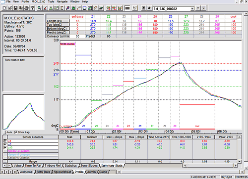 |
| FIGURE 13. Lead-free reflow profile. |
The first attempt using air reflow, however, showed unsatisfactory results. Poor wetting was evident and it was possible to see the sphere structure of the paste particles under microscope, even though the solder joints had verifiably experienced 235°C during reflow.
After this discovery, nitrogen was used to create an inert nitrogen atmosphere during reflow. The residual level of oxygen was stabilized at ~45 ppm. The next board reflowed showed excellent wetting and no further defects were observed, with every solder joint thoroughly inspected.
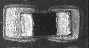
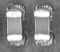
Post-reflow inspection. Post-reflow inspection was done manually under microscope and the result was judged according to workmanship standard IPC-A-610C. In the initial experiment, SnPb paste with ENIG finish were reflowed in air, and the wetting was good. This was however a very limited preliminary test and only 20 parts were reflowed and inspected; no defects were found. Figure 14 shows two typical samples from this batch.
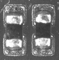 |
| FIGURE 14. Dummy 01005 capacitors assembled and reflowed in air on pad A, using Paste A. |
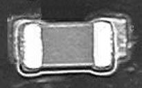
The components assembled in the initial trial were also inspected with x-ray (Figure 15) for voiding or other anomalies. The amount of voiding is not considered excessive. Both visual inspection and x-ray confirm that self-centering occurs when wetting is good. In Figure 16, the smooth surface of the SnPb solder joint is evident. In this trial, the paste printing process was not fully optimized, thus some fillet size variation can be seen.
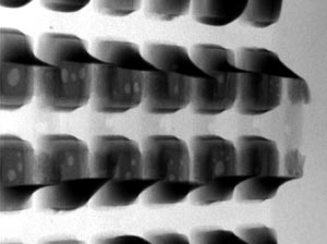 |
| FIGURE 15. Dummy 01005 resistors assembled and soldered in air on Pad B, using Paste A. |
 |
| FIGURE 16. Dummy 01005 resistors assembled and reflowed in air on Pad A, using Paste A. |
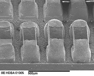
For the second set of experiments using OSP finish and lead-free solder, the 816 parts reflowed in air all had defects due to poor wetting. As seen in Figure 17, wetting is insufficient and the paste deposits have not formed a homogenous solder joint. No other defects were observed within this batch. Note that an optimized reflow profile that resulted in good wetting with larger solder paste deposits was used and the temperature was verified with calibrated equipment. The 800 parts reflowed in nitrogen had no defects at all, and the wetting was good (Figure 18). This difference is believed to be due to the small size of the solder paste deposits exposing most of the solder alloy particles to the surface, resulting in the loss of flux activity prior to reaching peak temperature during reflow in air.
 |
| FIGURE 17. Dummy 01005 capacitors assembled and reflowed in air on pad C, using Paste B. |
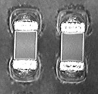 |
| FIGURE 18. Dummy 01005 capacitors assembled and reflowed in nitrogen on pad C, using Paste B. |
The visual inspection result and the defect levels indicate that pad layout C has been correctly designed. The wetting problem in air might possibly be solved with further optimization of solder paste, reflow profile and board coating, thus eliminating the need for nitrogen, but this remains to be seen.
Cross-sections analysis. Cross-sections were prepared using standard metallographic techniques. The sectioned samples (Figure 19) were inspected using light and SEM. Solder volume variation is again visible, as is solder voiding in the bondline region.
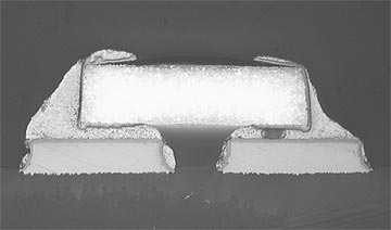 |
| FIGURE 19. Dummy 01005 resistors assembled and reflowed in air on Pad B, using Paste A. |
Shear testing. A shear test was performed on samples from the initial trial with the 01005 resistors. In this batch, SnPb solder and ENIG board finish were used. The load rate for the shear test was 500 µm/sec, and the shear height was 50 µm. All shears resulted in mixed mode failures (Table 3), including cracked ceramic, termination separation and solder shearing. n
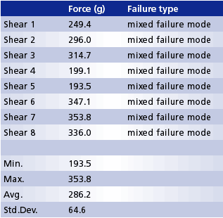 |
| TABLE 3. Shear test results from Pad B, Paste A. |
Ed.: This paper was originally published in the SMTA International Conference Proceedings, September 2004, and is used with permission.
Acknowledgments: The authors would like to thank Ninh Vu and Alington Lewis at Flextronics (San Jose, CA) for their assistance in the experimental work.
Bibliography
- D. Shangguan, “0201 Assembly Capability for Miniaturization: From Design to Volume Manufacturing,” Proceedings of 2003 International Printed Circuit & Electronics Assembly Fair Technical Conference and Exhibition, December 2003.
- D. Geiger, F. Mattsson, D. Shangguan, M. Ong, P. Wong, M. Wang, T. Castello and S. Yi, “Process Characterization of PCB Assembly Using 0201 Packages With Lead-Free Solder,” Soldering & Surface Mount Technology, 2003. (Also, Nepcon West Proceedings, December 2002.)
- D.A. Geiger, M. Wang, D. Shangguan, T. Castello and F. Mattson, “Reliability Study of Solder Joints for 0201 Components,” SMTA International Conference Proceedings, September 2003.
- M. Wang, D. Shangguan, M.T. Ong, F. Mattsson, D. Geiger and S. Yi, “Assembly Process Qualification on 0201 Packages for Volume Manufacturing,” SMTA International Conference Proceedings, September 2002.
- M. Wang, D. Shangguan, D. Geiger, F. Mattsson and S. Yi, “PCB Design Optimization of 0201 Packages for Assembly Processes,” SMTA/IMAPS Telecomm Hardware Solutions Conference & Exhibition Proceedings, May 2002.
- M. Wang, D. Shangguan, D. Geiger, K. Nakajima, C.C. Ho and S. Yi, “Board Design and Assembly Process Evaluation for 0201 Components on PCBs,” Apex Proceedings, January 2002.
- M. Wang, D. Geiger, K. Nakajima, D. Shangguan, C.C. Ho and S. Yi, “Investigation of Printing Issues and Stencil Design for 0201 Package,” SMTA International Conference Proceedings, October 2001.
, , and are with Flextronics (flextronics.com); dongkaishangguan@flextronics.com.


Press Releases
- Javad EMS Upgrades Through-Hole Soldering Capacity with New SEHO PowerWave System
- Sharpen Your Selective Soldering Skills with Kurtz Ersa's July VERSAFLOW 4/55 Training
- Omron Advances Inspection Technology with NVIDIA Omniverse and Metropolis
- Seika Machinery’s SMI 2026 Webinar Series Continues with Focus on PCB Cleaning Before Solder Paste Printing