

One Scan, Multiple Acoustic Images Per Component
Scanning multiple depths at once saves time and gives more accurate data at each depth.
A JEDEC tray filled with components of a single type is moved onto the stage of an automated acoustic microimaging system. The transducer begins scanning the tray, pulsing ultrasound into the components thousands of times a second and receiving the return echoes. Analysis of the echoes will identify components having internal anomalies that disqualify them from use. At the end of the line, those components will be removed.
This basic procedure is well known. Less well known is that an automated acoustic microimaging system can make multiple images of each of the components in the tray in the same scan time. The images of each component are analyzed – again, with no increase in time – and rejected components removed. The multiple-image approach is typically used on components where critical features exist at multiple depths that might complicate analysis if a single depth were scanned. Scanning multiple depths in the same scan gives more accurate data at each depth and simplifies analysis.
This method makes it easier for users to compare the acoustic data and images for a given lot of components to the standard used for that component. The standard, especially if it is based partly or entirely on the user’s experience with a component, is likely to be very specific in its accept/reject criteria. If significant internal features lie at multiple depths, scanning to produce a single-depth image may make analysis more difficult because the observer cannot tell, for example, whether a void is on top of the die paddle or a safe distance above it.
A pulse of ultrasound launched into the component by the transducer at a given x-y location travels through the mold compound at around 3,000 meters per second. The pulse is reflected only by material interfaces: the interface between the mold compound and the die face, for example, or between the mold compound and a lead finger. At any interface where both materials are solids, a portion of the ultrasound is reflected, and the remainder is transmitted across the interface deeper into the component, where it may encounter another material interface and repeat the process.
But if a gap such as a void or delamination exists between two solid materials – even if the gap is only a fraction of a micron thick – virtually all the ultrasound is reflected back to the transducer. None crosses the delamination or void. Many of the internal structural anomalies that will eventually lead to electrical failures in components during their service life are air-filled gaps, but a gap that is a vacuum or filled with another gas will behave the same way.
The transducer is positioned several millimeters above the component’s surface during scanning. The distance from the component’s surface to the depth of interest may be a millimeter or less. A pulse of ultrasound can thus be launched by the transducer, can enter the component, be reflected by a material interface, and return to the transducer in a few millionths of a second. This speed is what enables the system to evaluate several thousand x-y locations per second, and to assign to each echo from each location a pixel color within the acoustic image of the component.
Return echoes are nearly always gated, meaning only those echoes that arrive at the transducer within a specified time frame are used for imaging. When only a single image is needed at each x-y location, the gate includes the primary depth of interest. If a particular plastic-encapsulated microcircuit, for example, tends to fail because of voids between the die face and mold compound, then a vertically narrow gate may be used that may extend only 20µm or so above and below the interface. Many components use somewhat wider gates that are still less than the total thickness of the package. The widest gates are typically used on multilayer ceramic chip capacitors, where 1) a void or delamination at any depth can be lethal; and 2) the relative absence of local internal features makes defects easy to spot in the acoustic image.
Producing multiple images during a single scan can be performed by setting multiple gates. Suppose a given component may have significant defects at four separate depths. When the return echo begins to arrive from a single x-y coordinate, that portion of the echo arriving between 0.300 and 0.340ns, for example, is assigned to the first gate. The portion arriving between 0.340 and 0.380ns becomes the second gate, and so on. The gates typically have the same duration (vertical width), but they can be different widths, can be separated from each other, and can number 100 or more.
FIGURE 1 is an image of the die region of a plastic BGA assembly. This is gate 8 out of a total of 20 gates, which extend from just below the top surface to the substrate. Each gate is 50µm in vertical extent.
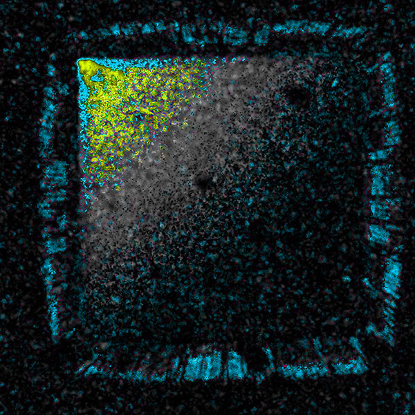
Figure 1. Gate 8 (of 20) catches only the highest corner of a tilted die.
One corner of the die is visible at the top left, but the rest of the die still lies below this gate and is partly or entirely out of focus. This tells the viewer the die is tilted, and thus may not be a good candidate for trouble-free service. If the tilt is severe enough, some wires may already be broken.
The next 50µm gate is shown in FIGURE 2. More than half the area of the die surface lies within this gate. The circular features of various diameters are voids in the mold compound. The voids may or may not be in physical contact with the die surface, but they are certainly very close to it.
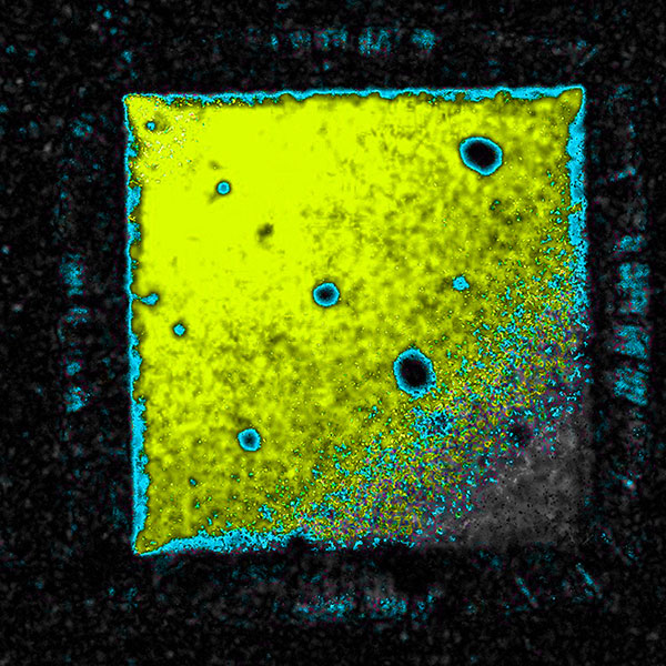
Figure 2. Gate 9 reveals most of the rest of the die, plus voids.
FIGURE 3 shows the deepest region of the die surface. Overall, the die slopes downward from top left to lower right. Since it occupies vertically part or all of three 50µm gates, the greatest corner-to-corner height difference is probably around 100µm.
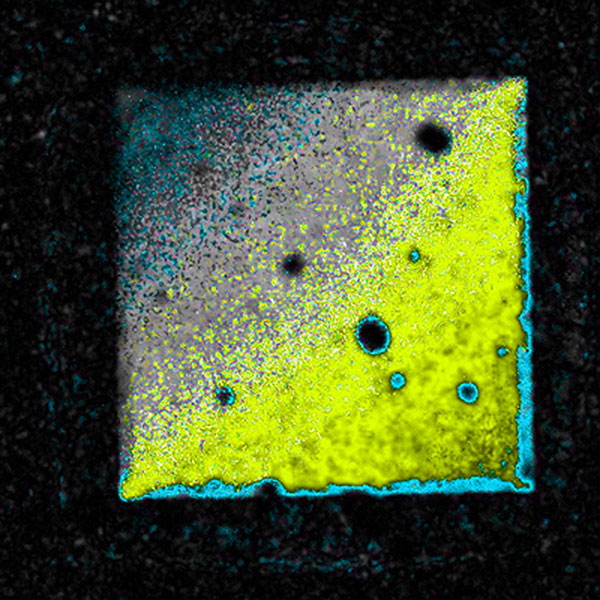
Figure 3. Gate 10 completes the picture and displays higher voids as shadows.
In the yellow region of this image are a few voids, with the blue outline and dark center seen in voids in Figures 1 and 2. But many of the voids seen in Figures 1 and 2 appear here as vague black forms without yellow outlines. They now lie above gate 3, and ultrasound reflected from the surface is locally blocked by these voids. Therefore, they appear as acoustic shadows.
What this sequence of images makes clear is the die is tilted. If viewing a single gate, it would likely have been set extending from well above the die face to below the die paddle, in order to catch any flaws within this critical range. Such a view would likely have shown the die as a flat feature, with nothing to indicate it is tilted. Using multiple gates showed its real posture.
FIGURE 4 shows the bulk scan image of a small area of a JEDEC tray used to scan a large number of plastic-packaged ICs. The purpose of imaging was to find structural defects by gating on the most critical depth, which in these components extends from just below the top surface of the part to the die paddle.
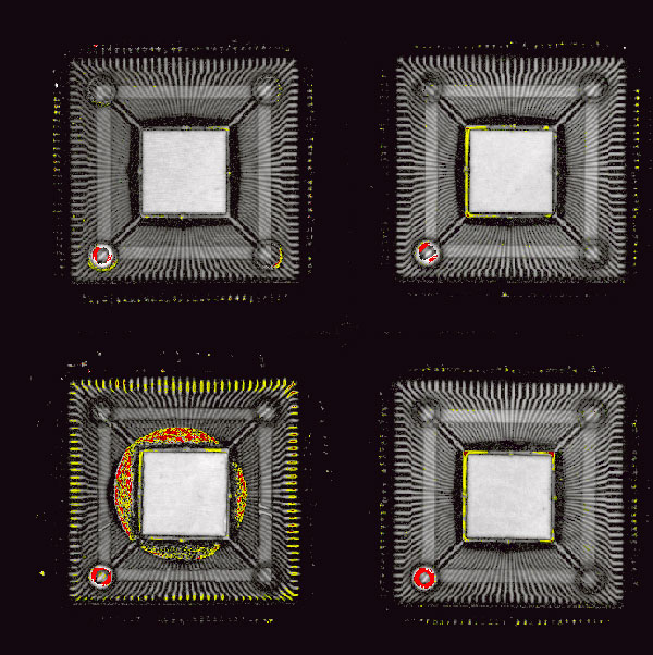
Figure 4. Bulk scanning of one corner of a JEDEC tray revealed only the popcorn crack at lower left.
The device at lower left has an obvious popcorn crack, as well as delamination at the distal ends of some of the lead fingers. The other three parts have no obvious internal defects.
The problem here is ultrasound pulsed into the component could not reliably send back usable echoes from the full thickness of the depth of interest. The mold compound appears a bit lossy, and other factors may make bulk scan less than ideal for finding defects at all depths.
The same portion of the JEDEC tray was then scanned with novel multi-focus imaging software using a total of 10 gates over the same distance from just below the top surface to the die paddle. The results are shown in FIGURE 5, the multi-focus image of gate 9.
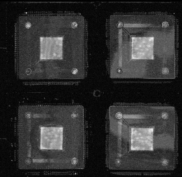
Figure 5. Gate 9 uncovered die attach voids in all four components.
In the part at lower left – the one with a popcorn crack – small, vague circular features are within the die area. At this depth, they can only be voids in the die attach. They are somewhat indistinct, perhaps because they lie partly within another gate. The other three components in this group show similar defects, none of which were visible in the bulk scan.
What differentiates the novel multi-focus imaging software from bulk scanning is each image is received separately and imaged separately (as in Figure 5), without having image data from higher depths displayed on top of it (as in Figure 4). When critical defects may lie at multiple depths, it is a very useful imaging mode.
is a consultant to Nordson Sonoscan (nordsonsonoscan.com); info@nordsonsonoscan.com.


Press Releases
- Seika Machinery’s SMI 2026 Webinar Series Continues with Focus on PCB Cleaning Before Solder Paste Printing
- Forwessun Expands Testing Capabilities through Strategic TRI Alliance
- Federal Electronics Expands Advanced Manufacturing Capabilities to Support Military and Aerospace Cable Assembly and Wire Harness Programs
- Altus Continues Irish Growth with Expansion of Engineering Team