

Can Tomorrow’s A&D Designs Handle the Heat?
New 3-D technologies with robust interconnects and thermal solutions are on the way.
Ed.: This is the fifth of an occasional series by the authors of the 2019 iNEMI Roadmap. This information is excerpted from the roadmap, available from iNEMI (inemi.org/2019-roadmap-overview).
Aerospace and defense (A&D) products face several challenges unique to this particular market segment, including the extreme environments in which they operate, need for security, desire for reworkability, long duration storage requirements and the functional lifetime over which the products are expected to perform and be supported.
The critical issues for the A&D sector can be reduced to a list of 11 challenges that need to be resolved for efficient manufacture and reliable use of current and emerging commercial off-the-shelf (COTS) technologies in military form factors on military platforms. These are:
- Affordability
- Mitigating any risks associated with Pb-free products
- Thermal management
- Weight and size reduction
- Increases in PWB density and complexity
- Reliability and associated ruggedization of COTS technologies
- Anti-tamper implementation
- Component availability, obsolete part strategies
- Configuration control
- Testability (and reworkability)
- Component authenticity (counterfeit concerns).
The industry’s move to Pb-free electronics poses several issues for A&D products. These include: 1) the long-term reliability of Pb-free solder alloys, 2) potential for tin whiskers and the required risk mitigation options, and 3) logistical issues associated with the declining availability of Pb-based components, configuration control, and depot and OEM maintenance and repair issues. Most A&D companies have at least a short-term strategy of continuing to provide Pb-based products while their supply chain is transitioning to Pb-free. Many customers are requiring formal Pb-free control plans (LFCPs) to protect against the unintended intrusion of Pb-free materials into their products. LFCPs require formal process changes that will, when implemented, identify any Pb-free finishes or solder alloys in the product’s design, assess its risk to performance and reliability, identify appropriate risk mitigation controls, implement controls that mitigate the risks, flow-down control requirements to the supply chain, and monitor incoming materials. One mitigation approach, for example, used by many military OEMs is to reball Pb-free BGAs with eutectic SnPb solder balls. This is an expensive approach.
Availability of components with either traditional eutectic SnPb solder balls or without solder balls would be simpler, but limited A&D volumes disincentivizes the component producer or drives greatly increased costs (and associated consistency risks) for a low-volume “defense-custom” alternative.
In A&D products, heat associated with power dissipation has traditionally been handled by passive conduction. The typical thermal path is from the component to the heat sink frame through “wedge locks” to the chassis. In the future, these conventional thermal management techniques will be inadequate. Improvements are required to reduce the thermal resistance across the wedge lock. Air and liquid “flow through frames” will be required, or changes that permit conduction cooling. These changes will require a significantly colder thermal interface for the assembly that is not always practical. These new thermal management designs must be assessed for their impact to interconnect reliability, testability and reworkability.
Component changes that increase the maximum allowable junction temperature would simplify board layout from a thermal perspective. However, the issues associated with thermal management may still become the biggest single roadblock to using some emerging technologies.
Uprating of commercial components is one method to meet thermal challenges, but not always affordable. Improvements in the thermal management approach and both bulk and interface materials will be required. Nanotechnology material improvements are needed to reduce thermal resistance at the component interface. These improvements will not only reduce the operational temperature of components, but also improve product MTBF and its expected service life. Work is ongoing to produce electronics that can withstand very high temperature operation, but cost, maturity and reliability concerns are still being addressed. The deep well industry is a source of new work in this area due to the extremely high-temperature environment.
Weight is extremely critical to the lifecycle cost of space and avionics systems. Weight reductions provide greater range, greater payload capacities, and significantly reduce operational cost of the platform. While significant opportunities reside with the platform structure, there are many additional opportunities in the domain of the electronic assemblies. It is anticipated both weight and size of MIL/AERO products will continue to decrease. Use of lightweight composite materials, including evolving nanotechnology materials, to replace conventional metals must continue to be evaluated, tested, and implemented. In many cases these materials provide not only weight reductions but also improvements in other critical areas such as thermal management. These opportunities need research and must mature to high-technology and high-manufacturing readiness levels. Expansion of 3-D technologies with robust interconnects and thermal solutions compatible with A&D product constraints is one area where weight and volume savings will be realized in the next few years.
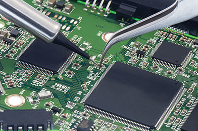
Figure 1. A&D customers want COTS parts, but many aren’t ruggedized or pose reworkability issues.
Continued evolution is required at the PWB level to permit circuit routing of emerging array components. These design, material and process changes need to be defined, developed, tested, and implemented. In some cases, requirements for digital and RF PWBs are converging. Most PWBs currently have surface-mounted components attached to both top and bottom surfaces. This has roughly doubled the board wiring density. Many new design features common to leading-edge high-density commercial products will be required for military products. Microvias (including via-in-pad) are required to facilitate wiring of high I/O fine pitch area array components, and multiple layers of stacked microvias are also needed to achieve the proper electrical performance for high frequency and increasing wiring density. These features will become more prevalent over the roadmap period. Electrical performance will drive signal integrity requirements, resulting in the need for improved impedance control and power integrity distribution requirements, which in turn will require embedded capacitance layers. In general, PWBs will have smaller plated through-holes; finer lines and spaces; a variety of buried, blind and microvias; and contain multiple types of laminate materials, each providing a unique function (i.e., capacitance, resistance, thermal dissipation). Recent automotive electronics developments involve place and embedding of 01005 and 0201 discretes within a PCB.
A&D customers require and expect COTS components and assemblies. Many of these technologies are not, as procured, demonstrated as capable of performing in harsh military environments for long periods of time. Pb-free initiatives make this challenge more complex. Tools and models are needed to identify when ruggedization is required and to validate its adequacy. The design modifications must be producible, of minimal impact to testability and reworkability, and affordable.
Anti-tamper (AT) and counterfeit avoidance, particularly malicious-intent counterfeit component and material insertion, is being increasingly required to prevent or at least delay exploitation of critical technology on military systems. Implementation of AT will require development of unique materials that can be applied within a secure infrastructure. Technology cycles and obsolescence continue to be a challenge to A&D products. Fundamentally, A&D products are developed for a specific customer, whereas COTS products are developed for a general market.
In many cases, the time to develop a product to a military customer’s specification and then perform some level of qualification testing (even highly accelerated life testing) is long in comparison to the planned lifecycle of its COTS components. There may be instances where COTS components become obsolete before the system goes into production. In addition, the designer must take into consideration the issue of spare parts availability and support over a typical military product lifespan of 10 to 30 years. Procuring end-of-life components increases the risk of counterfeits. Typical A&D products require both forward and backward traceability and stringent control of material and process change. This is not typically as closely controlled with COTS products. Again, with the transition to Pb-free components, configuration control of procured PCB assemblies and systems is more complex than in previous roadmaps.
A&D products require significant environmental stress testing prior to final customer sell-off and delivery. These tests consist of “shake and bake” testing, where the product in its final configuration is electrically tested over both accelerated temperature cycling and vibration that simulate a small portion of its operational life in the field environment. Prior to this phase of the production process, assemblies are conformal-coated and all thermal management completed (heat sinks attached, thermal interface materials added, etc.). It is critical that any problems detected at this level be diagnosed quickly to the component level for repair. To facilitate this, the design and test strategy must enable detection of issues as early in the manufacturing process as possible, where both fault isolation and repair are simpler. This emphasizes the importance of optimizing the test strategy relative to in-circuit or flying probe test, boundary scan test, and various emulators that permit increased levels of functional testing earlier in the manufacturing process. For failures detected at the final environmental screening, however, it is important to accurately and quickly diagnose the failure and be able to rework or repair product efficiently.
The issue of counterfeit parts is common to the entire electronic products domain, so it is certainly an issue to A&D products. The obsolescence issues associated with the production lifecycle, and certainly the sustainment phase of A&D products, magnify the issue. As described earlier, controls must be in place to avoid exposure to counterfeit parts, detect any suspect parts, and mitigate the risks of receiving counterfeit parts. New U.S. government rules levy the liability directly on the OEM for counterfeit parts in their products from any level in their supply chain. This ruling is being enforced, and the consequences are dire enough that an entire industry related to counterfeit part detection is rapidly expanding.
of Aeromarc LLC chaired the Aerospace//Defense Product Emulator Group (PEG) chapter of the 2019 iNEMI Roadmap.


Press Releases
- Seika Machinery’s SMI 2026 Webinar Series Continues with Focus on PCB Cleaning Before Solder Paste Printing
- Forwessun Expands Testing Capabilities through Strategic TRI Alliance
- Federal Electronics Expands Advanced Manufacturing Capabilities to Support Military and Aerospace Cable Assembly and Wire Harness Programs
- Altus Continues Irish Growth with Expansion of Engineering Team