

State-of-the-Art Technology Flashes
Updates in silicon and electronics technology.
Ed.: This is a special feature courtesy of Binghamton University.
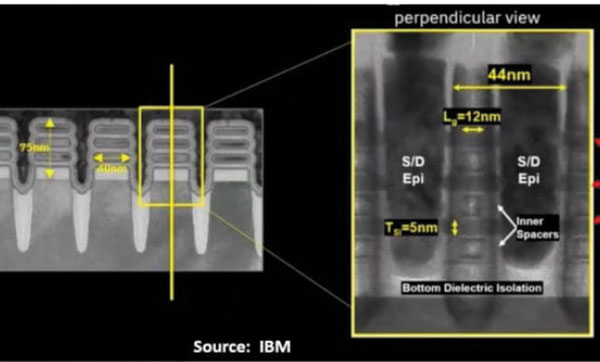
IBM announces 2nm GAA-FET technology. IBM announced its 2-nanometer CMOS technology, developed at its Albany research center. The development has technical firsts: the use of bulk Si wafers with bottom dielectric isolation under the nanosheet stack; reducing leakage and enabling 12-nnm gate lengths; a second-generation inner spacer dry process for precise gate control; FEOL EUV patterning to allow nanosheet widths from 15 to 70nm; and a novel multi-Vt scheme. This technology is expected to give a 45% performance boost or 75% power reduction, compared with the 7nm. (IEEC file #12324, Semiconductor Digest, 6/11/21)
Light-based method creates 2-D polymer. Linköping University researchers developed a method that uses light to manufacture 2-D polymers that have the thickness of a single molecule and could create a path for the development of ultra-thin, functional 2-D materials with highly defined crystalline structures. Using an on-surface photo-polymerization process, they tested a way to manufacture a 0.5nm-thick, 2-D polymer consisting of several hundred thousand molecules identically linked. The two-step method takes advantage of the self-organizing properties of fluorinated anthracene triptycene molecules. Because the polymerization takes place in a vacuum, the material is protected from contamination. The 2-D polymer film is stable under atmospheric conditions. (IEEC file #12370, Photonics Spectra, 7/14/21)
To continue reading, please log in or register using the link in the upper right corner of the page.


Press Releases
- Seika Machinery’s SMI 2026 Webinar Series Continues with Focus on PCB Cleaning Before Solder Paste Printing
- Forwessun Expands Testing Capabilities through Strategic TRI Alliance
- Federal Electronics Expands Advanced Manufacturing Capabilities to Support Military and Aerospace Cable Assembly and Wire Harness Programs
- Altus Continues Irish Growth with Expansion of Engineering Team