Optimizing Solder Paste Printing
Effects of varied keep-out distances for 0201 and 0402 components.
The trend toward smaller chip components and finer pitches on IC packages means smaller volumes of solder paste are required on each pad if problems of tombstoning, mid-chip balling and bridging are to be avoided. However, in most of these assemblies, there are also large components that require substantial volumes of solder to form joints with the required electrical and mechanical properties. For some components and finishes, extra solder paste is needed to compensate for potential coplanarity issues. Given the constraints on the area ratio, if an adequate transfer efficiency is to be achieved, the extent to which the solder paste volume can be controlled by varying the aperture dimensions is limited.
While there is hope that alternative application methods will make it possible to optimize solder paste volume for each pad, for the time being, the most cost-effective solution is to use a step stencil in which stencil thickness is varied to fine-tune the paste volume to the requirements of the component terminations. This solution imposes a constraint on the layout to the extent that components with similar requirements for solder paste volume have to be grouped. However, a greater concern in assemblies, in which space is at a premium, is the “keep-out” distance required on either side of the step.
Large keep-out distances used to accommodate various stencil thicknesses represent a significant loss of area available for component mounting. In this first project of iNEMI Asia, the objective is to determine for a representative range of components what the minimum distance on each side of the step can be without compromising the quality of the reflowed solder joint.
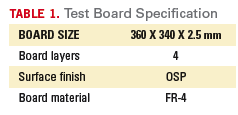
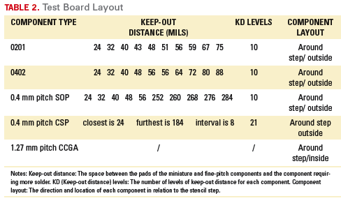
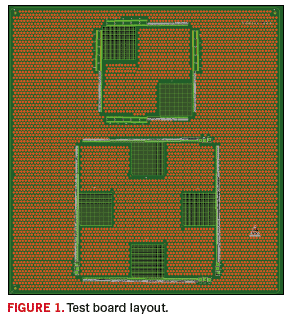
Test board specifications are listed in Table 1. The keep-out distance for step stencils has been described in IPC-7525. For the purpose of this project, boards were designed to provide a range of keep-out distances for 0201, 0402 and 0.4 mm pitch SOP and CSP components (Table 2). To assess the effect of printing direction, components were arranged around all four sides of the stepped area.

Experiment Matrix Design
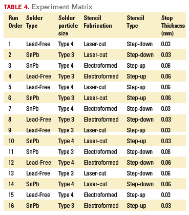
Given the project objective of determining the minimum keep-out distance that can be used in practical application, the experimental program covers a range of process variables typically encountered in commercial production (Table 4).
Experimental Procedure
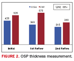
OSP thickness measurement. OSP finish solderability is known to be affected by the copper roughness and its ability to survive a reflow profile. It is known that OSP thickness may vary due to copper roughness. FIB was used to measure OSP thickness, since this method can accurately reveal the relationship between OSP thickness and copper roughness.
Figure 2 shows results of OSP thickness measurements on CCGA and CSP initially, and after the first and second reflow. The greater initial thickness of the OSP on the CSP pads is thought to be due to their smaller size. After the first reflow, there is not sufficient loss of coating thickness to compromise solderability, even on the copper peaks where the coating is thinner. After the second reflow, there is significant loss of coating thickness, but there is still sufficient coating on the peaks to protect the overall pad solderability, so that it is not expected solderability will be a factor influencing results in the later assembly stage of the project.
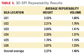
GR&R. GR&R was performed to determine the repeatability of the solder paste inspection equipment before starting the experiment. It was considered that results should be consistent within 10% of the measured value. A single board was printed and then inspected nine times, and the deposit height and volume results for BGA pads summarized in Table 5. The repeatability was calculated as follows:
Repeatability = 6 *σ/ (0.8 * average value)
Where σ = standard deviation of 9 samples
Average value = the average value of 9 samples
0.8 presents ± 40% process window
The repeatability was found to satisfy the set criterion (Table 5).
Printing parameter settings. Initial settings for print speed, squeegee pressure and separation speeds on a Speedline Accela printer were those recommended in the solder paste data sheet. Adjustments were then made on the basis of transfer efficiency, deposit shape and cleaning of the stencil surface, with the final settings listed below. To avoid any variation due to squeegee stroke direction, only the front to rear direction was used.
For runs 1-4:
- Print speed 75 mm/sec
- Squeegee pressure 8 kg
- Separation speed 5.5 mm/sec
- Separation mode Continuous
For runs 5-16:
- Print speed 35 mm/sec
- Squeegee pressure 8 kg
- Separation speed 5.5 mm/sec
- Separation mode Continuous
These settings were kept constant for all the remaining run orders (stencils) with careful checking of print quality after each stencil change. To enhance statistical significance, there were three repeats of each run order; a total of 48 boards were printed, with every pad inspected by 3-D SPI. Solder paste transfer efficiency and consistency were also recorded for analysis.
Data Analysis
DoE run. The DoE analysis was performed on each component surrounding the steps. These components are 0402, SOP, CSP, and 0201. The DoE analysis of 0402 is presented here as an example.
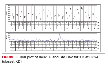
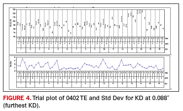
The 0402 component had 10 levels of KD. The closest, KD1, was 0.024˝. The furthest, KD10, was 0.088˝. Trial plots of 0402 data at each KD, grouped by DoE run order, orientation and side, indicate that ORT has a significant effect on TE (transfer efficiency) and deposit height, while the side does not have such a significant effect where:
- RO is run order.
- ORT is orientation of the component direction in relation to the step. ORT1 means the left and right side of the step, while ORT2 means the top and bottom side.
- Side is the side of the step. For example, ORT1 Side1 means the left side of the step.
Figures 3 and 4 are examples of such trial plots that represent the two extremes of KD. It can be seen that the TEs are almost the same for Side 1 and Side 2 for each run, but that there is a significant difference between ORT1 and ORT2 for most runs. This means ORT should be a separate factor, but the data of both sides may be able to be combined to simplify the DoE analysis.
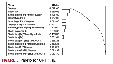
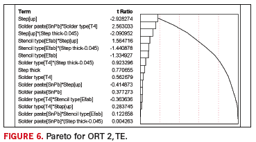
Among the five main DoE factors and the ten possible two-factor interactions, step appears to be the most significant factor in determining TE for both ORT1 (Figure 5) and ORT2 (Figure 6). The next most significant factors appear to be step height for ORT1 (Figure 5), and then solder paste and solder type combinations (Figure 6).
KD trend analysis. The line plot, which directly presents the trend for each run and differences between runs, was also used in the analysis of the results. Transfer efficiency and consistency will be particularly considered here, and results for 0402 are again used as examples.
Figure 7 shows the line plot of TE for 0402:
KD is not the significant factor in a single run, which means TE varies little with increasing KD;
TEs differ between some runs, especially Runs 13 and 14, which have TE values higher than other runs.
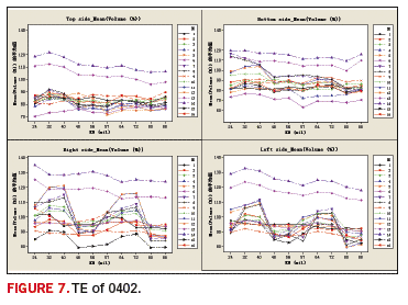
Figure 8 shows the line plot of transfer consistency for 0402:
KD is not the significant factor in a single run, which means TC varies little with increasing KD
TC differs little between runs, but Run 10 is an exception;
There is a large variation in TC for all 16 runs on the left of the step at 0.056˝ KD. The cause has been the subject of discussion by the project team and attributed to differences in the stencil fabrication.
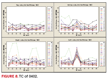
Table 6 summarizes the analyses of 0201, 0.4 mm pitch CSP and SOP components using this method.

First Stage Summary
Based on this analysis, the following conclusions have been drawn:
While it might be expected on the basis of common sense that the farthest KD should yield a better TE and deposit height than the closest KD, the trend analysis shows the KD has little or no effect on TE and height for 0402 and SOP type pads. Variations between DoE runs are greater than variation with the KD over the range studied.
For all keep-out distances and run orders, orientation has a significant effect. ORT1 (aperture at the side of step) always gives higher TE than ORT2 (aperture at the front/rear of the step). But with the same orientation, side has little or no effect.
From the overall DoE analysis, the project team saw the following factors as important:
- Solder paste type.
- Stencil type.
- Step down/up.
- Step thickness.
- That was expected, and confirmed the team had chosen the right factors and/or level setting.
An unexpected result was some DoE runs yielded TEs significantly different from others. The cause of this excessive swing in the response variable is unknown at this point; more investigation by the team is needed to understand and explain the cause.
Based on the results of the first stage printing experiments, assembly verification was planned. Finally the optimum keep-out distances for each component type in various applications will be obtained.
Acknowledgment
The authors appreciate the close cooperation between Huawei, Alcatel-Lucent, Speedline, Indium Corporation, IST, Cisco, Rohm & Haas, Nihon Superior, Celestica and iNEMI on this project, and extend their thanks to Photo Stencil and all the engineers involved for their great support.
The iNEMI Solder Paste Deposition Group is Shoukai Zhang, Huawei; Rita Mohanty, Ph.D., Speedline; Xiaodong Jiang, Alcatel-Lucent Shanghai Bell; Runsheng Mao, Ph.D., Indium; Chiko Yu, Integrated Service Technology; Chuan Xia, Cisco Systems; Keith Sweatman, Nihon Superior; Desmond Teoh, Celestica; and Haley Fu, Ph.D., and Jim Arnold, Ph.D., iNEMI.
Press Releases
- Koh Young Webinar to Show How Data Transparency Strengthens SMT Production Resilience
- Aven Welcomes Max Ramos to Strengthen Distribution Partner Operations
- ubersmt Expands SMT Line with Juki G-Titan Printer and RS-1R Placement System
- Keiron Technologies to Host LiFT Webinar Focusing on Solving Solder Paste Printing Challenges


