Automated Testing with Boundary Scan
Boundary scan’s low-cost and IC level access has pushed its use beyond traditional board test applications.
Boundary scan is a method for testing interconnects on PCBs or sub-blocks inside an integrated circuit. It has rapidly become the technology of choice
for building reliable high technology electronic products with a high degree of testability.
Boundary scan, as defined by IEEE Std. 1149.1 developed by the Joint Test Action Group (JTAG), is an integrated method for testing interconnects on PCBs that are implemented at the IC level. The inability to test highly complex and dense printed circuit boards using traditional in-circuit testers and bed-of-nails fixtures was evident in the mid 1980s. Due to physical space constraints and loss of physical access to fine pitch components and BGA devices, fixturing cost increased dramatically, while fixture reliability decreased at the same time.
The boundary scan architecture provides a means to test interconnects and clusters of logic, memories, etc., without using physical test probes. It adds one or more so-called “test cells” connected to each pin of the device that can selectively override the functionality of that pin. These cells can be programmed via the JTAG scan chain to drive a signal onto a pin and across an individual trace on the board. The cell at the destination of the board trace can then be programmed to read the value at the pin, verifying the board trace properly connects the two pins. If the trace is shorted to another signal or if the trace has been cut, the correct signal value will not show up at the destination pin, and the board will be known to have a fault.
When performing boundary scan inside ICs, cells are added between logical design blocks to be able to control them in the same manner as if they were physically independent circuits. For normal operation, the added boundary scan latch cells are set so they have no effect on the circuit, and are therefore effectively invisible. However, when the circuit is set into a test mode, the latches enable a data stream to be passed from one latch to the next. Once the complete data word has been passed into the circuit under test, it can be latched into place. Since the cells can be used to force data into the board, they can set up test conditions. The relevant states can then be fed back into the test system by clocking the data word back so that it can be analyzed.
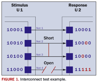
The principles of interconnect test using boundary scan are illustrated in Figure 1, depicting two boundary scan-compliant devices, U1 and U2, which are connected with four nets. U1 includes four outputs that are driving the four inputs of U2 with various values. In this case, we will assume the circuit includes two faults: a short between Nets 2 and 3, and an open on Net 4. We will also assume a short between two nets behaves as a wired-AND, and an open is sensed as logic 1. To detect and isolate the above defects, the tester is shifting the patterns shown in Figure 1 into the U1 boundary scan register and applying these patterns to the inputs of U2. The input values of U2 boundary scan register are shifted out and compared to the expected results. In this case, the results (marked in red) on Nets 2, 3, and 4 do not match the expected values and, therefore, the tester detects the faults on Nets 2, 3 and 4.

By adopting this technique, it is possible for a test system to gain test access to a board. As most of today’s boards are very densely populated with components and traces, it is very difficult for test systems to access the relevant areas of the board to enable them to test the board. Boundary scan makes this possible.
Debugging. While it is obvious that boundary scan-based testing can be used in the production phase of a product, new developments and applications of IEEE-1149.1 have enabled the use of boundary scan in many other product lifecycle phases. Specifically, boundary scan technology is now applied to product design, prototype debugging and field service.
A large proportion of high-end embedded systems has a JTAG port. ARM [Advanced RISC (reduced instruction set computer) Machine] processors come with JTAG support, as do most FPGAs (field-programmable gate arrays). Modern 8- and 16-bit microcontroller chips, such as Atmel AVR and TI MSP430 chips, rely on JTAG to support in-circuit debugging and firmware reprogramming (except on the very smallest chips, which don’t have enough pins to spare and thus rely on proprietary single-wire programming interfaces).
The PCI (Peripheral Component Interconnect) bus connector standard contains optional JTAG signals on pins 1 to 5; PCI-Express contains JTAG signals on pins 5 to 9. A special JTAG card can be used to re-flash corrupted BIOS (Basic Input/Output System). In addition, almost all complex programmable logic device (CPLD) and FPGA manufacturers, such as Altera, Lattice and Xilinx, have incorporated boundary scan logic into their components, including additional circuitry that uses the boundary scan four-wire JTAG interface to program their devices in-system.
ACI Technologies Inc. (www.aciusa.org) is a scientific research corporation dedicated to the advancement of electronics manufacturing processes and materials for the Department of Defense and industry. This column appears monthly.
Press Releases
- Horizon Sales Adds High-Speed PCB Testing with Takaya Flying Probe Systems
- Distron Adds Second Shift, Expanding Capacity to Support Around-the-Clock Production
- Horizon Sales Expands Consumables Portfolio with ROCKA Partnership, Bringing More Value to U.S. Manufacturers
- Libra Industries Appoints Gustavo Sariñana as General Manager of Guaymas Facility


