

Defluxing of Copper Pillar Bumped Flip-Chips
A case study showed a well-balanced aqueous cleaning agent removed Pb-free, water-soluble tack flux residues better than straight DI water.
Solder bump technology is problematic below 150µm pitch, since it is challenging to manufacture and assemble. As the bump pitch size shrinks, solder bumps have many limitations in the fine-pitch process. Bump printing, plating or bump drops, along with bump pad sizes, are the major constraints; as a result, risk of shorts increases. Today, dies in production have as many as 25,000 bumps per die. It has been predicted this number will increase to 50,000 to 60,000 per die in the next year or two.1
Another form of bump gaining more popularity is the copper pillar. These bumps, instead of being spherical in shape, are in the form of a pillar, with various shapes and sizes. The most popular shape is in the form of a cylinder. The pillar shape allows the high ratio of bump height to bump diameter, therefore permitting very tight pitch, even when bump heights are large. Sometimes a solder cap is formed on top of the pillar to help with connectivity with the mating chip.1 Due to the cylindrical shape and non-collapsing nature of Cu pillar bumps, they can be easily mounted on the fine trace of the laminate. Copper pillars are terminals used to flip-chip IC chips to a substrate in a semiconductor package by thermal compression flip-chip (TCFC) technology. Copper pillars are formed on aluminum electrode pads of an IC chip.
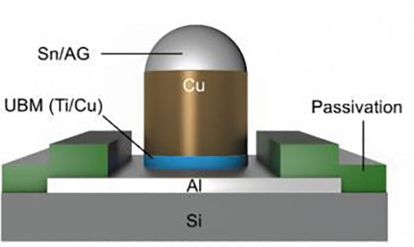
Figure 1. Copper pillar bump typical structure.
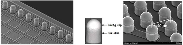
Figure 2. SEM image of Cu pillar bumps.
The bump height can vary anywhere from 5µm to 100µm and diameter from 10-20 to 100µm and larger. Most pillar bumps now in production are larger than 20µm in height. FIGURE 3 shows a representative picture of miniaturization of traditional Pb-free and Cu pillar bumps for fine-pitch flip-chip applications.2
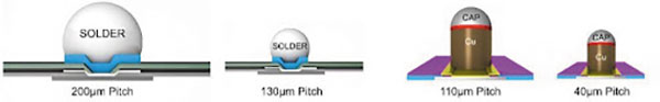
Figure 3. Flip-chip bump miniaturization typical data.
The use of copper pillar technology for flip-chip represented about 25% of the market in 2013, increased to over 50% by 2020, and is projected to make up about 80% of the flip-chip market by the end of 2024. Copper pillar is likely to become the most dominant type of flip-chip interconnect in the coming years.3
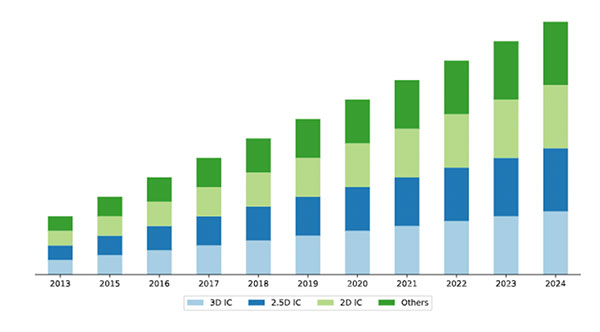
Figure 4. Historical and forecast growth of copper pillar technology within the flip-chip market.
Copper pillar technology has been well documented to be efficient down to 80µm pitch and appears to be a promising approach down to 30µm pitch. Along with reduced pitches, copper pillar brings other benefits, including superior electromigration performance for high current carrying capacity applications, improved thermal conductivity, simplified under-bump metallization (UBM), and higher I/O density. Also, it can be used for extreme fine-pitch-on-silicon package devices down to 40µm for through silicon via (TSV) and chip on chip (CoC).
Packages using copper pillar bumps have more interconnects per surface area, resulting in tighter pitch and lower standoff gaps. As standoff gap reduces, flux residues have less area to outgas during reflow. This results in more active residues under the die.
Flux residues can affect reliability in two ways: First, on the solder bump, substrate or die, thin films of flux residue can significantly reduce interfacial adhesion between the flux and the surfaces. Once the underfilled device is stressed by thermal shock, humidity or other factors, the underfill delaminates from the surface, and a gap can be detected using acoustic microscopy; second, fluxes can also affect reliability by physically impeding the flow of underfill material. Flux residue buildup in the gap between bumps or between the die and the substrate can narrow the gap to a point where the underfill cannot flow, or the edges flow faster, encapsulating air and creating a void. To ensure a void-free underfill, homogenous wetting of the underfill must occur on all surfaces. If wetting is not homogenous, voids in the uncured underfill may translate into reliability problems later.4
Most copper pillar applications rely on cleaning with deionized (DI) water only for OA flux removal. Numerous studies already conducted suggest water is beginning to reach its cleaning limitation, however, favoring use of aqueous processes.5, 6, 7 Increased use of Pb-free solder, which typically requires higher soldering temperatures, is one reason. This results in more burned-in fluxes that are much harder to remove as they begin to produce water-insoluble contamination. DI water alone has limited to no ability to solubilize nonionic residues on the board surface.
Second, cleaning water-soluble fluxes, especially under components, has grown more difficult. In other words, water, with its high surface tension of more than 70 dynes/cm, cannot remove flux residues under bump pitch less than 40µm.
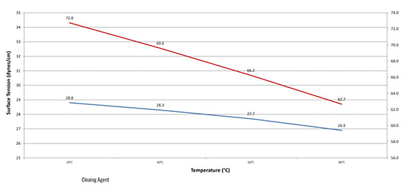
Figure 5. Surface tension values.
Aqueous is a term that implies the use of aqueous-based chemistry: for example, an application concentration of 15% mixed with DI water. The level of active concentration actually is secondary; however, aqueous implies the addition of aqueous ingredients. Aqueous cleaning agents diluted in deionized water significantly reduce the surface tension, providing better cleaning through lower ionic contamination, which in turn provides higher product reliability. These cleaning agents are pH-neutral to mildly alkaline in nature, having corrosion inhibitors as part of their formulation, exhibiting full compatibility with a variety of metals (Sn, Ag, Cu, Ni, Al, etc.) present on the copper pillar die. Lack of corrosion inhibitors can easily attack these metals, causing galvanic corrosion reactions.
This study explores the impact of flux cleaning using DI water and a well-balanced aqueous cleaning agent on copper pillar bumped flip-chips. The scope is limited to copper-pillar bumped flip-chips having pitch of 150µm. This study enables the authors to determine the wash parameters and conditions required to effectively clean flux residues underneath these components to ensure reliability and functionality of the final product.
Results are verified via analytical test (IC, SEM/EDS and FTIR) and reliability test methods, including thermal cycling, high temperature storage life (HTSL) and moisture sensitivity level 3 (MSL-3) testing.
The outcome of this study can be used as a benchmark for conducting further studies involving bump pitch less than 15µm and denser packages, including 2.5-Ds and 3-Ds.
Material Specifications
Substrate specification. The substrate used in this study was organic-based with a thickness of 960µm, having a daisy-chain function. The core material was E-679FGR using PSR4000-AUS703 solder resist. The surface finish on the pads was electroless nickel/immersion gold (ENIG).
Wafer specification. An 8" wafer was selected with a base oxide layer composed of plasma-enhanced tetraethyl orthosilicate (PE-TEOS) and TiN/Al-0.5%Cu metal layer composition. The passivation layer was a combination of high-density plasma/plasma-deposited SiN (HDP/ P-SiN), and the metallization selected was TiCu/Cu. The bump material was Cu/Sn-2.5Ag.
Chip specifications. In this study, 10mm x 10mm flip-chip with a daisy-chain structure was used. Cu pillar was designed with 150µm bump pitch and a 30µm Cu pillar height. The pad size was 100µm square with the bump size of Φ75µm. There were a total of 3,721 pads/chips.
- Chip size: 10mm x 10mm
- Number of pads: 61 x 61 = 3,721 pads/chips
- Pad size: 100µm square
- Pitch: 150µm
- Passivation opening: Φ 80µm
- Bump height: Cu 30µm + SnAg 15µm
- Bump size: Φ 75µm
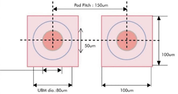
Figure 6. Chip specification.
The geometry of the copper pillars used in a test vehicle are shown in (FIGURE 7).
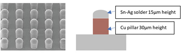
Figure 7. Copper pillar geometry.
FIGURE 8 shows a cross-section of copper bump.
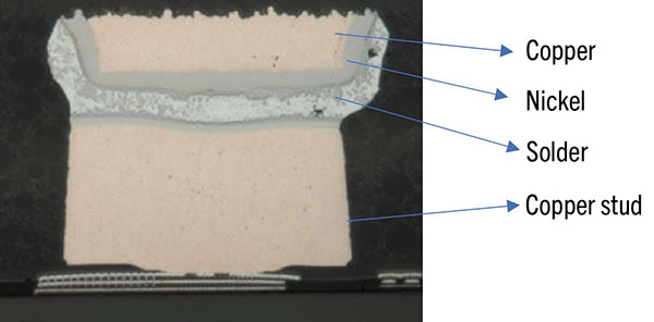
Figure 8. Cross-section of copper bump.
Flux specification. The flux used in this study was a Japanese Pb-free water-soluble tacky flux, one of the most commonly used materials in semiconductor packaging, including copper pillar bump applications. The staging time between reflow and cleaning at chemical supplier site was 24 hr., representing a worst-case scenario.
Assembly process. The assembly process requires proper optimization of chip placement on the substrate to get an optimized solder profile. For that reason, it was decided to collaborate with Universal Instruments Advanced Process Lab, which has the capability to assemble and perform reliability testing. The die and substrates were sent to the UI lab for assembly. Die placement was performed using a Universal Instruments’ FuzionSC platform.
The water-soluble tacky flux was applied using a linear thin-film applicator (LTFA), which is an on-board dipping process that provides maximum efficiency to facilitate the wetting of the solder bump. The LTFA creates a thin film of flux, solder paste or adhesive. The packages are individually or gang-dipped, thereby applying the necessary amount of material to the appropriate area. It uses a plate about 38µm thick to create a film.
X-ray inspection. Post-placement, inspection was done using x-ray to ensure the bump was aligned properly to the pad. First article inspection (FAI) was conducted using x-ray prior to chip placement on the remaining lot, and necessary adjustments were made to align the die.
Reflow profile. The package was reflowed using a Pb-free solder profile using a BTU Pyramax 125 10-zone convection reflow oven under nitrogen (less than 200ppm) with a peak temperature of 250°C (FIGURE 9). Several reflow profiles were evaluated until the heating and cooling rate was sufficiently controlled to get an optimum bump profile post-reflow and minimize stress on the reflowed bump. Open bumps can occur on the reflowed side or at the die-to-bump interface due to coefficient of thermal expansion (CTE) mismatch and substrate warpage during reflow.
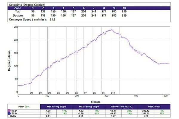
Figure 9. Reflow soldering profile used.
Equipment. A conveyorized spray-in-air inline cleaner was used for this study. FIGURE 10 shows a schematic of the inline cleaning system.
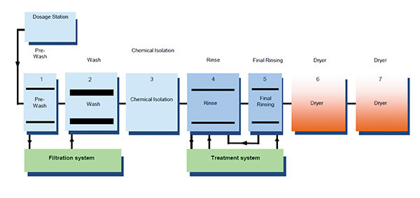
Figure 10. Schematic of conveyorized spray-in-air inline cleaner.
Cleaning agents. The cleaning agents included:
- Pure deionized water at 100% concentration (10 Meg-Ω resistivity).
- An aqueous-based cleaning agent specifically developed for the removal of Pb-free water-soluble fluxes from various package types, including those under test.
Experimental
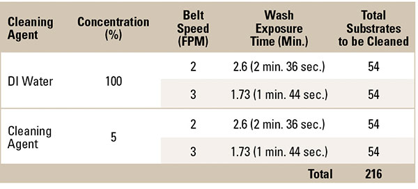
A total of 216 packages were built for this study.
Table 1. Test Plan Used in the Study
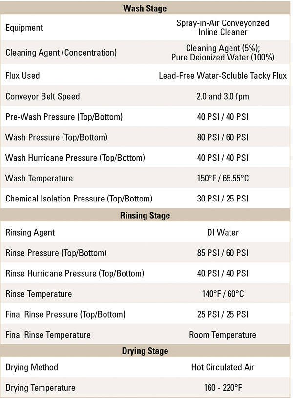
The process settings in TABLE 2 were used in the inline cleaner.
Table 2. Inline Cleaner Process Parameters
The cleaning trials were split into two groups to minimize the flux staging time and keep it the same. The first set of 108 substrates were processed and assembled at Universal Instruments and shipped overnight to the cleaning agent supplier to be cleaned with DI water. The second set of remaining 108 substrates were processed and assembled the following day and shipped overnight to be cleaned with the cleaning agent.
Post-cleaning, all the substrates were shipped immediately back to Universal Instruments for reliability testing. This included thermal cycling, high-temperature storage life (HTSL) and moisture sensitivity level 3 (MSL-3) test. The remaining cleaned substrates were subjected to analytical test (IC, SEM/EDS and FTIR).
TABLE 3 details the reliability/analytical test performed on the substrates cleaned with both deionized water and the cleaning agent.
Table 3. Reliability/Analytical Test Performed8, 9, 10, 11, 12
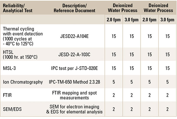
In addition, ion chromatography testing was performed on bare substrates (5 in total) and substrates having Pb-free water-soluble tacky flux (5 in total) to determine their cleanliness levels and ionic species.
Post-cleaning, the substrates were underfilled using a liquid epoxy encapsulant specifically formulated for tight bump pitch, and a narrow gap in flip-chip BGA applications was used. The process was carried out using an Nordson Asymtek Axiom X-1020 dispenser configured with an Asymtek DJ-9500 DispenseJet valve for noncontact jetting of precise volumes of fluid in dots, lines and patterns.
Reliability Test Results
A prerequisite to package reliability testing is moisture preconditioning to classify package MSL class and ensure it survives reliability test post-moisture soak. Packages were subjected to MSL-3 preconditioning at 60°C/30% RH for 192 hr., followed by 3x reflows at 260°C. The reliability tests results are summarized in TABLE 4.
Table 4. Reliability Test Results
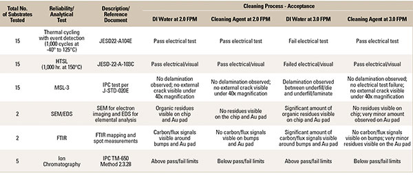
SEM/EDS/FTIR analysis. The goal of the analysis is to evaluate the overall cleanliness under the chip component, as well as surface cleanliness of the Au pad. Post-cleaning, the substrate was cracked, and both the chip and test substrate (Au pad) were analyzed using SEM/EDS and FTIR.
SEM/EDS analysis. SEM/EDS analysis was performed using a Zeiss Sigma 300VP and Oxford X-maxN 80. Over a period of 4.5 hr., the entire substrate surface was scanned at 200x magnification for a total of 667 individual pictures. These pictures were stitched together using Zeiss SmartStitch software. The BSE detector at 1.5kV was used in this study. The BSE detector is typically very sensitive to the presence of organic contaminations/residues (black = organics). It indicates the density of the material. Material with high density looks brighter (e.g., metals), and material with lower density looks darker (e.g., organics like flux residues).
FIGURE 11 is an example of stitched area of unclean copper pillar substrate (chip backside). The image consists of 300 individual pictures that were stitched together. The dark areas observed indicate the presence of organic flux residues.
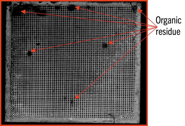
Figure 11. SEM imaging of unclean chip showing presence of organic flux residues.
Table 5. SEM Images for Unclean, DI Water and Cleaning Agent at 2.0 FPM
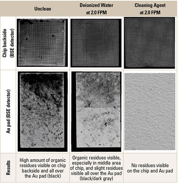
Table 6. SEM Images for Unclean, DI Water and Cleaning Agent at 3.0 FPM
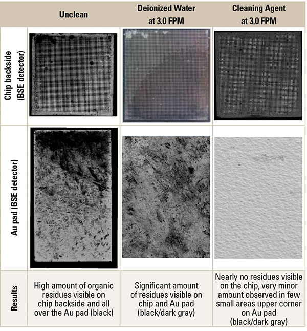
Table 7. EDS Images for Unclean, DI Water (at 2.0 FPM) and Cleaning Agent (at 3.0 FPM)
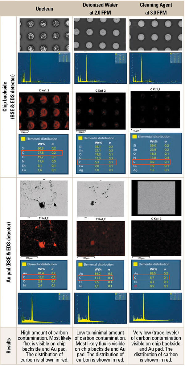
SEM/EDS overall results. Substrates cleaned with DI water showed the presence of organic residues on both the chip and the Au pad at 2.0 FPM. At an increased belt speed of 3.0 FPM, a significant amount of residues on both the chip and the Au pad were observed. In the case of the cleaning agent, 2.0 FPM did not exhibit any residues, whereas a minor amount of residues was seen on the Au pad at increased belt speed of 3.0 FPM. Overall, substrates cleaned with the cleaning agent showed a minimal amount of residues compared to “unclean” substrates and substrates cleaned with deionized water.
FTIR analysis. FTIR analysis was performed using Bruker LUMOS equipment. The spectrometer is equipped with a liquid-nitrogen-cooled detector. The measurements were performed in attenuated total reflection (ATR) mode.
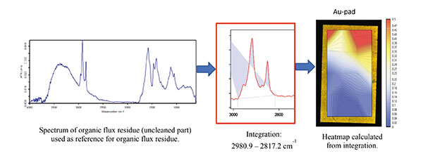
Figure 12. Example of FTIR heat map generation.
The Au pad surface was scanned with 20 measurement spots (each 125 x 125µm) in ATR mode. Via integration, it was determined the organic signal was in the range of 2980.9 - 2817.2cm-1. All the obtained 20 spots were converted into a heat map. The FTIR heat map indicates the intensity of carbon/flux contamination. As a reference, a flux spectrum was used. Red areas indicate high organic contamination, and blue areas indicate low to zero organic contamination. All spectras were corrected for CO2 (at around 2,400 to 2,200 cm-1).
TABLE 8. FTIR Results for Unclean, DI Water (at 2.0 FPM) and Cleaning Agent (at 3.0 FPM)
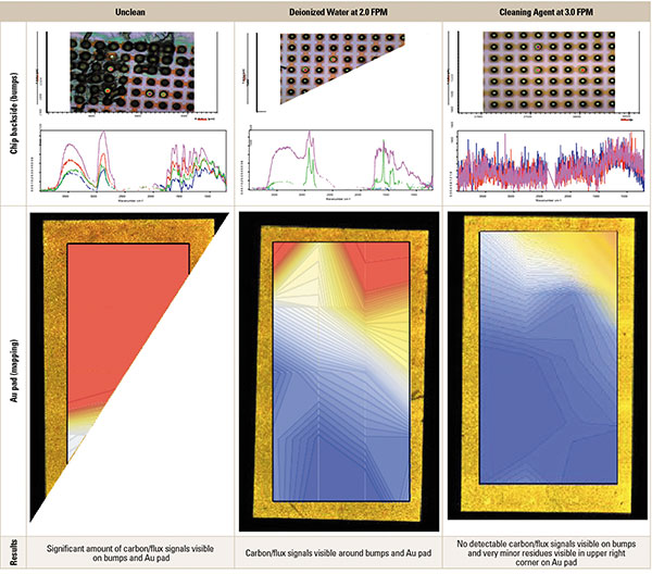
FTIR overall results. Substrates cleaned with DI water at 2.0 FPM exhibited a significant amount of residues on both bumps and Au pad. On the other hand, substrates subjected to the cleaning agent at 3.0 FPM did not exhibit any carbon/flux signals on the bumps. Very minor residues were observed on the Au pad in the upper right corner.
Overall, substrates cleaned with the cleaning agent showed a significant improvement compared to DI-water-cleaned substrates, even at faster belt speed.
Ion chromatography results. All the test coupons were subjected to ion chromatography analysis per IPC-TM-650, Method 2.3.28. IC analysis used an extraction solution of 10/90 v/v IPA/deionized water.
Table 9. Ion Chromatography Results – Bare Substrates
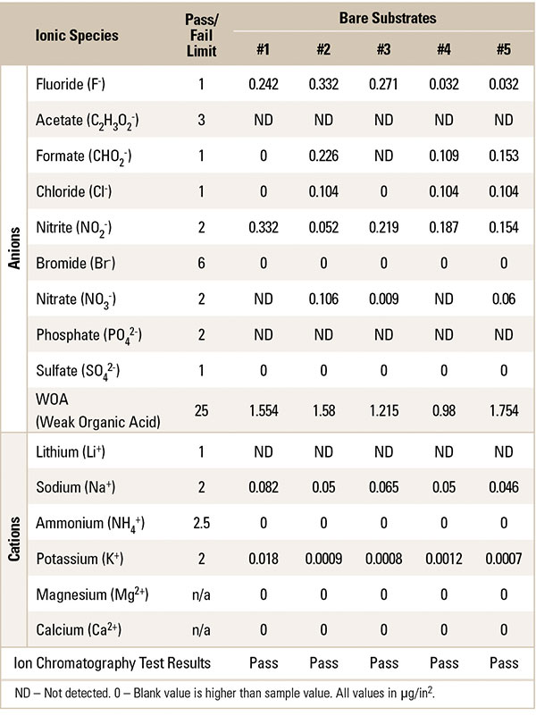
Table 10. Ion Chromatography Results – Unclean Substrates Having LF Water-soluble Tacky Flux Residues
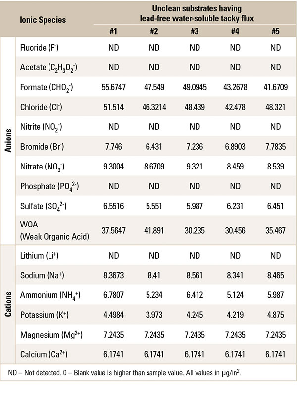
Table 11. Ion Chromatography Results – Substrates Cleaned with DI Water at 2.0 FPM
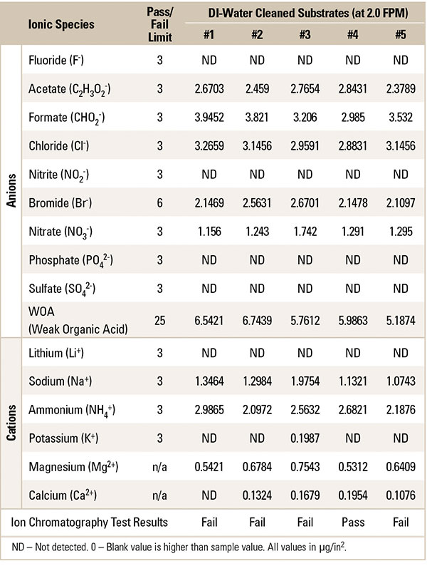
Table 12. Ion Chromatography Results – Substrates Cleaned with DI Water at 3.0 FPM
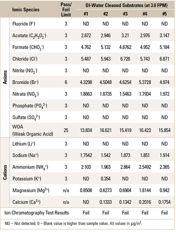
Table 13. Ion Chromatography Results – Substrates Cleaned with Cleaning Agent at 2.0 FPM
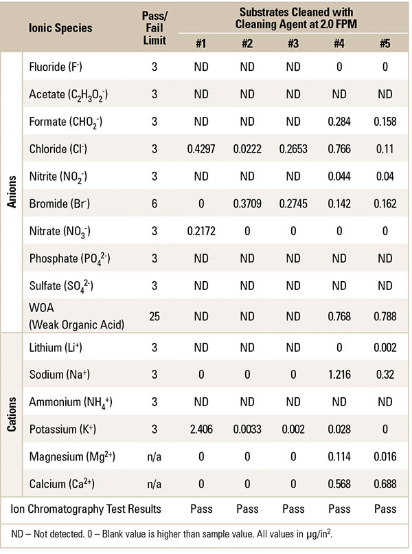
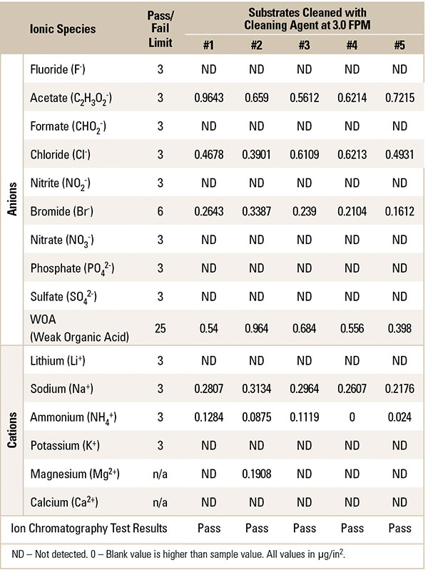
Table 14. Ion Chromatography Results – Substrates Cleaned with Cleaning Agent at 3.0 FPM
- All the bare substrates passed, exhibiting low levels of ionic species.
- Uncleaned substrates having Pb-free, water-soluble tacky flux residues showed significantly high levels of cations, anions and weak organic acids.
- DI-water-cleaned packages failed the IC test, exhibiting high levels of formate and chloride ions. At 2.0 FPM, even though substrate #4 passed the IC test, the values for formate ions were very close to pass/fail limits. At 3.0 FPM, significant failures were observed for acetate, formate and chloride ions.
- Substrates cleaned with the cleaning agent passed the IC test at both 2.0 and 3.0 FPM, with a majority of the ionic species below the pass/fail limits.
Conclusions
This comparative study confirmed the deionized water inline cleaning system is challenged to consistently and effectively clean flux residues underneath low-standoff components, especially when it comes to cleaning under copper pillar packages with 150µm bump pitch and 30µm Cu pillar height.
The DI-water-cleaned substrates at 3.0 FPM failed the thermal cycling, HTSL and MSL-3 test. Moreover, substrates cleaned with DI water exhibited the presence of carbon contamination on the chip backside and the Au pad via SEM/EDS/FTIR analysis, as well as high levels of ionic species when subjected to IC testing.
In comparison, substrates subjected to the cleaning agent passed the thermal cycling, HTSL and MSL-3 test. These packages showed better cleaning performance under chip component, as well as on the investigated Au pad. Very minor residue was visible when subjected to SEM/EDS/FTIR analysis. IC testing also showed very low levels of ionic species.
Based on the overall study conducted, it is observed the cleaning agent at low concentration (5%) may completely remove the Pb-free, water-soluble tacky flux residues at faster belt speed (3.0 FPM) compared to straight DI water at 2.0 FPM, which would also enable an increase in throughput of 50%.
It should be noted the copper pillar flip-chip substrates were cleaned 24 hr. after the assembly and soldering process. Generally, its recommended to clean the water-soluble tacky flux as soon as possible (preferably within an hour post-soldering).
Acknowledgments
The authors would like to thank the R&D team of Dr. O.K. Wack Chemie for continued guidance in this study. The authors want to express gratitude to the individuals at our partner companies that helped design the advanced packages, as well as for conducting reliability testing.
References
1. Rudolph Technologies, Inc., “Copper Pillar and Micro Bump Inspection Requirements and Challenges,” application note. www.circuitnet.com/news/uploads/1/Copper_Pillar_App_rev2.pdf.
2. N. Islam, V. Pandey, M. Hsieh and K. Taek, “Fine Pitch Cu Pillar Assembly Challenges for Advanced Flip Chip Package,” Proceedings of IWLCP Conference, 2017.
3. Market Intellica, “Global Copper Pillar Flip Chip Market 2019,” www.marketintellica.com/report/MI92620-global-copper-pillar-flip-chip-market.
4. P. Phoosekieaw and S. Khunkhao, “Flux/Inderfill Compatibility Study for Flip-chip Assembly Process,” Proceedings of 2011 International Conference on Information and Electronics Engineering, 2011.
5. H. Wack, U. Tosun, R. Parthasarathy and J. Patel, Limitations of DI-Water Cleaning Processes, Zestron case study.
6. J. Patel, R. Parthasarathy, U. Tosun and M. McCutchen, “Comparative Cleaning Study to Showcase Effective Removal of OA Flux Residues,” Proceedings of SMTAI, October 2012.
7. R. Parthasarathy and B. Bibeau, Water Soluble Flux Residue and Product Reliability … A Connection, Zestron case study.
8. J-STD-020E, Moisture/Reflow Sensitivity Classification for Nonhermetic Surface Mount Devices, February 2015.
9. Jedec JESD22-A104E, Temperature Cycling Test Procedure/Method, May 2005.
10. Jedec JESD-22-A-103C, High Temperature Storage Life Test Procedure/Method, November 2004.
11. IPC TM-650, Method 2.3.28.2, Bare Printed Board Cleanliness by Ion Chromatography, December 2009.
12. IPC TM-650, Method 2.3.28B, Ionic Analysis of Circuit Boards, Ion Chromatography Method, November 2012.
This paper was previously presented at IPC Apex Expo 2022 and is reprinted here with the authors’ permission.
, is senior application engineer at Zestron Americas (zestronusa.com); ravi.parthasarathy@zestronusa.com. , is application technology manager at Zestron Americas; umut.tosun@zestronusa.com.


Press Releases
- Altus Adds LPKF CuttingMaster 3290 to Depaneling Portfolio
- Kurtz Ersa Partners with E-tronix for Sales in Illinois and Wisconsin
- XLR8 EMS Welcomes Raul Jorge Lopez Jr. as Director of Program Management and Procurement
- Koh Young America Promotes Ramiro Mora to Lead Service and Applications in Mexico and South America