

RF Shield Rework
A new solution involves high-energy conduction heating and custom tips.
Radio frequency (RF) shields are used to separate areas of a printed circuit board (PCB) assembly from each other and to reduce noise and prevent radio signals from escaping from the product and affecting operation of other devices. Antenna products, cellphones and wireless electronics require RF shielding either mounted to the PCB or incorporated into the packaging that surrounds the electronics.
RF shield rework is difficult due to continually shrinking package sizes, reduction of pitch and reduced clear space available around components. This increased density and complexity drives new techniques for removing and replacing RF shields.
Shields are attached to PCBs via two common methods. Both methods attempt to completely cage a specific area by soldering to surface connections to ground planes internal to the PCB. In one method, a metallic “fence” is attached around the perimeter of the area to be shielded (Figure 1). A spring-loaded metallic “lid” is then snapped over the fence to enclose the area. The mechanical contact of the lid and fence creates the RF shield.
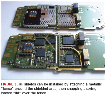
The fence can be added anywhere during the process before solder reflow. Typically, the fence is manually placed by machine using an odd form assembly system. The lid is manually placed after reflow or by a second automated system, and can be readily removed if components inside require replacement.
The second method is a one-step process that adds the shields during fine-pitch placement. By using one-piece shields presented in tape-and-reel or component trays, RF shield attachment requires no changes in the assembly process. The shields are placed and then soldered directly on the board using a standard reflow process. No additional operators or inline equipment are required. A complete metallic bond surrounding the entire area provides the most reliable RF shield and prevents the end-user from tampering with the device. However, if defective components are found during in-circuit or functional test, or if a device upgrade is called for, the shield must be de-soldered.
Three particular challenges need to be addressed:
- Removing the typically odd-shaped shields from the PCB.
- Restoring the proper volume of solder for new shield attachments. (Depending on the condition after removal, residual solder might need to be cleaned and sometimes can remain, with additional solder paste dispensed to add volume for new shield attachments.)
- Producing repeatable results without special operator skills.
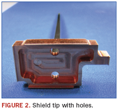
To remove the shield, the nozzle design must conform to the shield’s external shape. There are targeted points at which the shield is soldered to the PCB, and the nozzle needs to be designed so that heat is directed to these areas. This ensures the shield is consistently removed from the PCB without damage to either the board or shield. Attempting to remove the shield before the solder reaches its melting point will inevitably cause damage to the pads on the PCB and render the entire board useless.
Convection is a very common heat source for rework and repair purposes, but for the removal of RF shields, it is not an ideal solution. Creating a temperature adequate to remove these relatively high-mass metal parts without damaging surrounding components and the board itself presents a significant challenge.
Fixed temperature conduction heat. An appealing alternative demonstrating distinct advantages is high-energy conduction heating applied through custom-tooled thermal tips that match the shape of the shields.
When the novel heating element is energized by its high-frequency alternating current (AC) power source, the current automatically begins to flow through the conductive copper core of the heater. However, as the AC current continues to flow, a physical phenomenon known as the skin effect occurs1, and the current flow is directed to the skin of the heater assembly, driving the majority of the current through the high-resistance magnetic layer and causing rapid heating.
As the outer layer reaches a specific temperature (controlled by its heater alloy formula), it loses its magnetic properties. This “Curie point” temperature is when the skin effect begins to decrease, again permitting the current back into the conductive core of the heater and repeating the cycle.
Faster and safer removal. Successful shield removal applications have been demonstrated to reduce the heating time from as many as five minutes using conventional methods to under 45 sec., while keeping the components beneath the shield lid to <200°C. This is a critical concern with glued parts because adhesive expansion in the z axis can be extreme enough to tear the pads.
In Figure 3, the red plotted line shows solder on the shield melting above 217°C. The green and blue lines represent the parts under the shield. In the profile (Figure 3), the first time bar (1.19) shows the preheated time. The tip touches the shields when the PCB is at 84°C.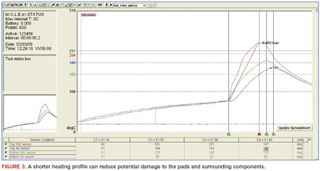
The peak is at 1.42 seconds, which means the contact time – the period the tip was on the shield – was 23 sec. (1.42 – 1.19).
Fixed temperature-variable energy direct conductive heating process provides fast, safe shield lid removal without the problems of adjacent reflow. The process shows potential for providing fast, efficient direct removal of BGA components by delivering heat directly though the component body perimeter and removing the unwanted device without surrounding reflow and risk of damage to the board or nearby components.
References
William Hayt, Engineering Electromagnetics, 4th edition, McGraw-Hill, 1981.
Paul Wood is advanced applications manager at OK International (okinternational.com); pwood@okinternational.com.


Press Releases
- XLR8 EMS Welcomes Raul Jorge Lopez Jr. as Director of Program Management and Procurement
- Koh Young America Promotes Ramiro Mora to Lead Service and Applications in Mexico and South America
- ViTrox Americas Welcomes Huy Pham as Technical Support Engineer
- XLR8 EMS Appoints Steve Dutton as Chief Sales Officer