

Tackling Head-in-Pillow Defects with Vapor Phase Reflow
An EMS finds VPS dramatically reduced HiP in BGA/LGA connectors.
Head-in-pillow (HiP) defects are one of the most common issues that affect printed circuit boards containing ball grid array/land grid array (BGA/LGA) packages. These defects can result in costly repairs and reduce a component’s lifespan. HiP defects are compromised solder joints often attributed to undesired environmental factors during the reflow process. These factors include reflow in an oxygen-filled environment, exposure to temperatures surpassing a component’s thermal limit, and uneven thermal distribution across the PCB.
Exploration of innovative reflow processes has led to the renewed adoption of vapor phase soldering within electronics manufacturing. Vapor phase soldering introduces an oxygen-free environment and a unique heating process that could address the cause of HiP defects. Collecting images and data from a reflowed BGA/LGA hybrid connector in a convection oven, then using vapor phase soldering (VPS) for rework, we investigated whether vapor phase reflow addresses this defect. The data showed a noticeable improvement in solder quality, as well as increased coplanarity after vapor phase rework. These findings offer preliminary support for the benefits offered when reflowing PCBAs using VPS.
BGA/LGA hybrid connectors function much like the human body’s nervous system. They permit the microprocessor – the brain – to interface with all other components on the PCBA. The sensitive digital cortex has a low tolerance for faults, and a PCBA without its brain is little more than some copper and silicon.
One common fault that threatens a system’s integrity is the head-in-pillow defect. These defects have become increasingly common with the adoption of lead-free alloys in BGA-style components. Although HiP defects can result in immediate intermittent failure of a PCBA, the more common outcome is a failure in the field due to moderate or thermal stress. The defects tend to form during the reflow process, and a few factors that often contribute to their formation include exceeding a component’s thermal limitations, the unequal distribution of heat during reflow, and exposing a component to an oxygenated environment. This less-than-ideal environment, and the subsequent development of HiP defects, has plagued the industry for years.
Before the late 1980s, the preferred reflow method was VPS because of its enhanced heat transfer capabilities.1 Speculation over its negative environmental impact, however, led to the abandonment of vapor phase technologies in mainstream electronics manufacturing. Modern innovations in the vapor phase reflow process have resulted in the adoption of perfluoropolyethers (PFPEs), which have a reduced environmental impact. This has caused a resurgence in the use of VPS in many industries, especially those with low tolerance for electrical failures.
The changes in the reflow process between convection and vapor phase put into question which process is more favorable regarding HIP defects. Research by Leicht and Thumm indicated the reflow environment observed when using VPS reduced the conditions that cause HiP defects.2 To investigate the impact of changing the reflow environment, a comparison was made between convection and vapor phase processes. The discrepancy between the two processes supports the conclusion that using vapor phase technology reduces HiP defects, addressing its key causes and making it an effective countermeasure.
The HiP Defect
As illustrated in FIGURE 1, head-in-pillow defects are mechanically weakened solder joints. These defects are most common on BGA/LGA-style packages. They often retain electrical integrity, which permits them to pass functional tests. Yet, they still result in in-field failures.4,5,6 These failures are due to mechanical or thermal stresses exerted on the defective component. Due to the nature of BGA packages, these defects can be costly.
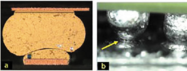
Figure 1. Example of a head-in-pillow defect where image A is the optical micrograph of a solder joint. This defect is likely caused by an oxide layer forming between the pad and lead. Image B is the side view of the HiP defect affecting a BGA solder ball.3
Many factors can result in HiP defects. One of the primary causes is the occurrence of a common solder defect known as poor wetting.4,5 This issue is often the result of oxidation during the soldering process. Oxidation is the chemical reaction between oxygen molecules and exposed metal that results in the formation of oxide layers. These layers cause imperfections in the solder joints that lead to the aforementioned defects. Traditionally, flux is used to break down these oxide layers, albeit without complete effectiveness.
Another factor that can cause HiP is warpage. Warpage is the deformation of the components or the PCB.5,8 Different materials expand at different rates when exposed to high temperatures. This is exaggerated if the heat is disproportionately distributed across the surface of the material.
As PCBs and components are soldered, they undergo a heating cycle that uses different temperature zones to gradually heat the PCBA. This can lead to uneven thermal distribution, as one end of the PCBA is heated before the other, subsequently leading to PCB warpage. The different temperature zones require a higher peak temperature, as the PCB must be held above the solder paste’s melting point for up to 30 seconds. This is often achieved by increasing the maximum applied temperature up to 35°C, per the solder paste manufacturer’s specifications. The use of this overhead is to ensure thicker PCBs and high-mass components reach and exceed the solder paste’s melting point.2 Applying peak temperatures of this magnitude disrupts the functionality of BGA/LGA-style packages due to the component’s internal material composition. These higher temperatures often exceed the limitations of the component, which cause it to unevenly expand and subsequently warp. As the PCB and/or component warp, the solder balls disengage from the pads. This leads to defective solder joints, as either oxides form in between the pad and ball, or the pad and ball cool at different rates and fail to form a proper solder joint (Figure 2). Both these effects lead to the creation of HiP defects.
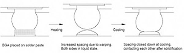
Figure 2. Diagram representing one cause of HIP defects. As the solder melts, the land pad and BGA ball disengage. After the solder starts cooling, they make contact again, yet do not form a bond.7
What is Vapor Phase?
Dr. Robert C. Pfahl at Western Electric developed the vapor phase reflow process in 1974.2 Widely used in the early ’80s, vapor phase reflow was the process of choice because of its exceptional thermal transfer characteristic. In 1987, around the time of the adoption of the Montreal Protocol, the technology was cast aside over environmental concerns. This policy banned the emission of chlorofluorocarbons (CFCs), which, at the time, were the favored chemical used for the vapor phase process. Infrared and convection ovens replaced vapor phase reflow in mainstream manufacturing. The process became limited to the production of more difficult assemblies, such as PCBAs with higher mass components or PCBAs with a mix of high- and low-mass components. Today, VPS has addressed the ban on CFCs and instead uses non-toxic PFPEs.2 The process is primarily found in industries with a low tolerance for defects, such as aerospace or defense.
The vapor phase reflow process, illustrated in FIGURE 3, works by using an inert chemical as a heat-conducting medium. The PCBA is placed in a chamber above the inert chemical, commonly Galden PFPE in liquid form. The Galden PFPE is then heated to form a layer of vapor that displaces the oxygen due to its higher density. The PCBA gets lowered into the vapor layer, permitting the vapor to encapsulate it. As the vapor contacts the PCBA, it forms a film of condensation. This film acts as a layer of protection against oxidation, while simultaneously conducting its thermal energy.2,9 The vapor continuously condenses, constantly renewing the protective film and further conducting heat. As the film encompasses the PCBA, it homogeneously transfers heat. The transfer of thermal energy to the PCBA is also more efficient, which permits manufacturers to employ a lower overhead temperature during reflow. Vapor phase has a max peak temperature dependent on the type of chemical used. This controlled peak temperature, coupled with an improved thermal transfer process, allows it to target the solder’s specified reflow temperature to within a couple degrees.2 Overall, this low temperature process reduces the risk of thermally sensitive components warping during reflow, especially BGA/LGA-style packages.
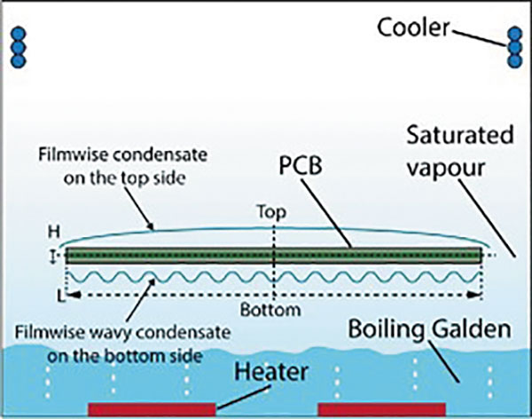
Figure 3. Diagram representing the process of vapor phase reflow. Vapor condenses to form a film around the PCBA, which protects it from oxidation. This film continues to be replaced as more vapor condenses. This process heats the board as the hot vapor undergoes conduction with the PCBA.10
VPS Effect on HiP
The major benefit of vapor phase reflow is its ideal soldering environment compared to that of the convection reflow process. Because this ideal environment is oxygen-free, it eliminates any chance of oxidation, while also permitting homogeneous heating of the PCBA. In traditional convection ovens, the PCBA is gradually heated as it passes through different temperature zones, which causes different parts of the board to experience unequal levels of heat. When using vapor phase reflow, the Galden PFPE film distributes heat evenly, which reduces the chance of warpage. Additionally, the process has a limited peak temperature due to the type of Galden PFPE used. This low-temperature solution is only viable as the heat transfer process is much more efficient and accurate with vapor phase reflow. Overall, this process addresses the primary environmental factors that cause HiP defects.
Experimental Methodology
To demonstrate the capabilities of vapor phase reflow, one can look to a real-world application of the process. A client requested services regarding an issue they encountered during PCBA manufacturing. Post-production, five to 10% of the batch of boards had a HiP defect, and the client wanted to rework the PCBAs. Vapor phase reflow was used to repair the defects, and a comparison, before and after the rework, reveals the differences between the processes. (The solder on the PCBA was RoHS-compliant and lead-free.)
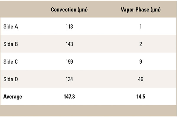
Starting with the convection reflow process, a PCBA containing a BGA/LGA connector was reflowed and, subsequently, developed HiP defects. Once it arrived in the facility, it underwent functional testing, which resulted in intermittent failures of the component. Images of the connector’s solder joints were taken, in addition to a delta height measurement. The delta height measurement is the difference between the height of either side of the component relative to the plane of the PCBA substrate (FIGURE 4). This measurement can be used as an indication of coplanarity and assist in the analysis of HiP defects. Data were recorded for each side of the connector (TABLE 1).
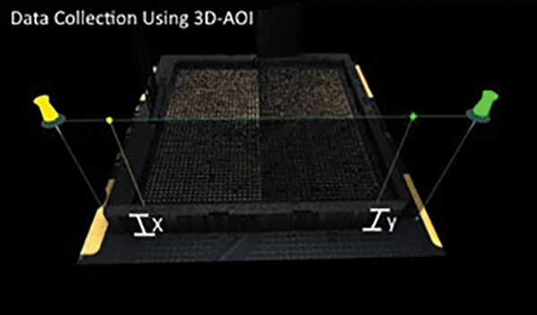
Figure 4. Image seen in 3-D AOI during inspection. Measurements x and y were taken relative to the plane of the PCB. Delta height is the difference between the x and y measurements. These measurements were repeated for each side of the BGA/LGA hybrid connector.
Table 1. Coplanarity Comparison
The defective BGA/LGA connector was then reworked using the vapor phase reflow process. Both images and delta height measurements of the reworked connector were taken and recorded. FIGURE 5 compares the difference in solder ball quality between the results from the convection reflow process and the vapor phase reflow process.
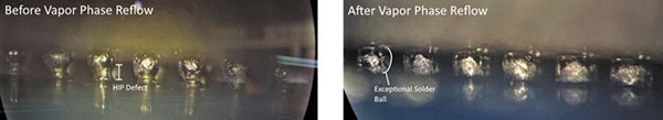
FIGURE 5. Two images of solder joints of a BGA/LGA hybrid connector. The left image is after the convection oven reflow with HiP defects. The right image is after the vapor phase rework. Inspection of the solder balls revealed elongated solder joints and HiP defects. After the rework, the solder joint formed an exceptional solder ball.
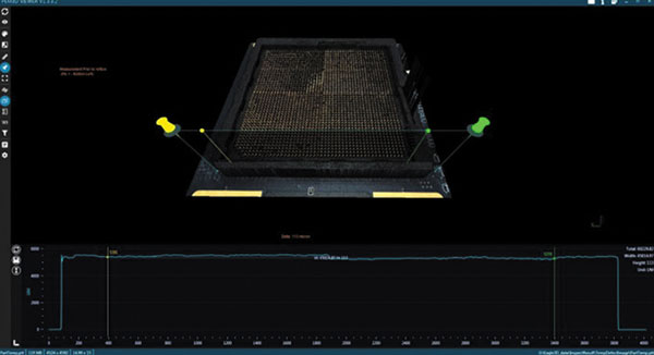
FIGURE 6. 3-D AOI rendered image of side A before rework. Calculations made by pins seen in image.
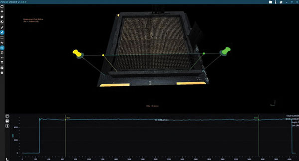
FIGURE 7. 3-D AOI rendered image of side A after rework. Calculations made by pins seen in image.
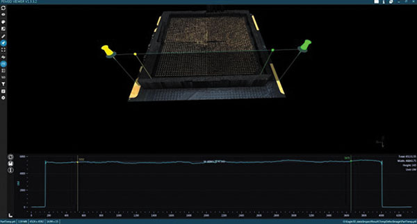
FIGURE 8. 3-D AOI rendered image of side B before rework. Calculations made by pins seen in image.
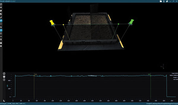
FIGURE 9. 3-D AOI rendered image of side B after rework. Calculations made by pins seen in image.
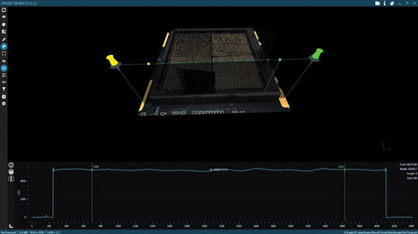
FIGURE 10. 3-D AOI rendered image of side C before rework. Calculations made by pins seen in image.
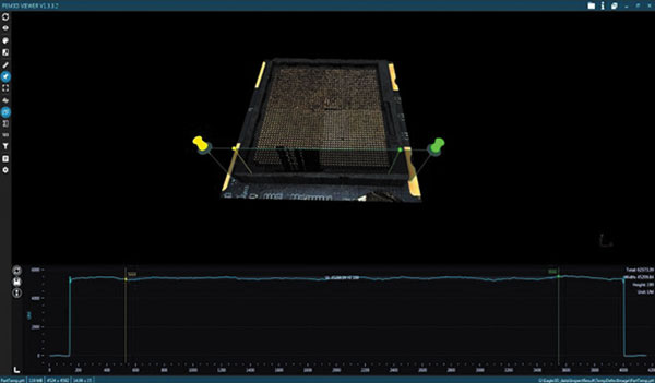
FIGURE 11. 3-D AOI rendered image of side C after rework. Calculations made by pins seen in image.
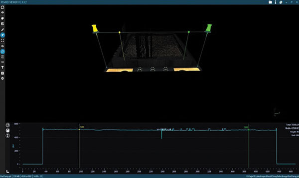
FIGURE 12. 3-D AOI rendered image of side D before rework. Calculations made by pins seen in image.
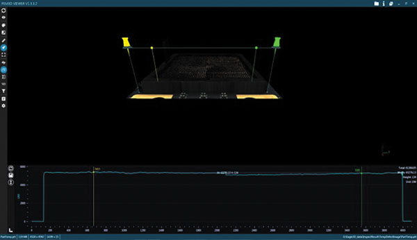
FIGURE 13. 3-D AOI rendered image of side D after rework. Calculations made by pins seen in image.
Data Analysis
When analyzing the data, the change in delta height was an indication of improvements in the solder ball quality and, therefore, the lack of presence of a HiP defect. From the results in Table 1, between the convection and vapor phase reflow processes, a large change is noted in the delta height for each side of the BGA/LGA connector. For example, through the convection process, Side A measured to be 113µm, whereas through the vapor phase process it was 1µm, a 112µm decrease in the delta height measurement.
Using these results, we calculated the average delta height of the components for each process. Overall, a difference of 132.8µm was recorded in the delta height – a 90.2% decrease, which indicates a drastic increase in coplanarity. A visual inspection of the solder balls after rework showed all solder bonds greatly improved. Functional testing revealed the component was operating as expected. These results can be attributed to the VPS process. The increase in coplanarity is likely a result of even heat distribution and low temperature peaks, which limits the warpage and permits concurrent solder bonding. The increased coplanarity assists in the reduction of HIP defects, as solder joints don’t stretch to connect leads to the PCB.
Limiting the stretching also reduces the amount of solder and pad that is exposed to oxidation. Along with limited exposure is the elimination of an oxygenated environment. The protection against oxidation enables an ideal reflow environment. Results indicate vapor phase reflow improved the reflow environment and eliminated HiP defects.
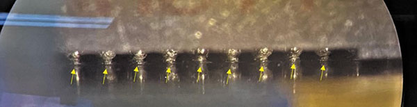
Figure 14. Side A solder balls before VPS rework.
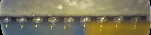
Figure 15. Side A solder balls after VPS rework.
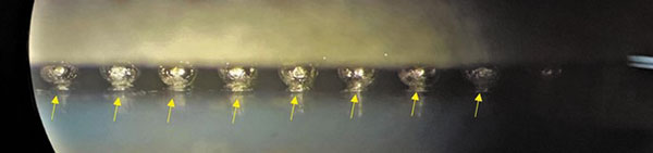
Figure 16. Side B solder balls before VPS rework.
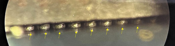
Figure 17. Side B solder balls after VPS rework.
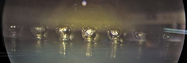
Figure 18. Side C solder balls before VPS rework.
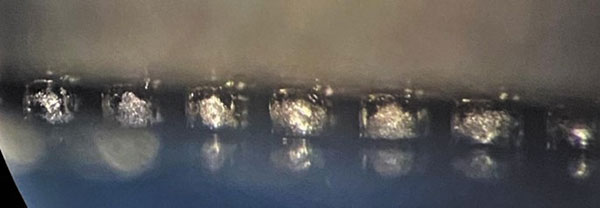
Figure 19. Side C solder balls after VPS rework.
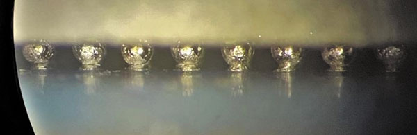
Figure 20. Side D solder balls before rework is done by vapor phase soldering.
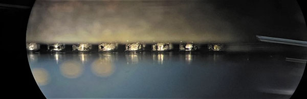
Figure 21. Side D solder balls after rework is done by vapor phase soldering.
Conclusion
Using data collected during the rework of a defective BGA/LGA hybrid connector, we analyzed attributes of vapor phase soldering that benefit the manufacturing of PCBAs. The oxygen-free environment, low temperature process, and even heat distribution emulate an optimal reflow environment. This environment is extremely useful in tackling head-in-pillow defects both during the manufacturing and rework of PCBAs. The ability to rework and prevent these defects ensures the longevity of electrical devices and lessens constraints placed on PCB designers. Vapor phase reflow is a promising solution to the dreaded HiP defect. •
References
1. A. Samat and K. Chia, “Reintroduction of Vapor Phase Soldering Technology for Lead Free Application,” SMTA International, 2009, https://www.circuitinsight.com/pdf/reintroduction_vapor_phase_soldering_smta.pdf.
2. Dipl.-Ing. Helmut Leicht and A. Thumm, “Today’s Vapor Phase Soldering an Optimized Reflow Technology for Lead Free Soldering, https://smtnet.com/library/files/upload/Vapor-Phase-Soldering.pdf.
3. R. Nowland, “Telecommunications Studies Address Head-in-Pillow (HnP) Defects and Mitigation Through Assembly Process Modifications and Control,” IPC Apex, 2010, https://www.semanticscholar.org/paper/Head-in-Pillow-(-HnP-)-Defects-and-Mitigation-and-Nowland/cee46d59969a0d8de3761748cd3d80b197e1fcfd.
4. K. Seelig, “Head-in-Pillow BGA Defects,” white paper, 2009, https://aimsolder.com/sites/default/files/head-in-pillow_bga_defects.pdf.
5. C. Oliphant, B. Christian, K. Subba-Rao, F. Doyle, and Dr. L. Turbini, “Head-On-Pillow Defect – A Pain in the Neck or Head-On-Pillow BGA Solder Defect,” IPC Apex Expo 2010, https://www.circuitinsight.com/pdf/head_pillow_defect_ipc.pdf.
6. J. Nguyen, “Mitigation of Head-in-Pillow Defect,” June 2017, https://www.circuitsassembly.com/ca/magazine/27514-soldering-1706.html.
7. Dr. N.-C. Lee, D. Y. Liu, and P. F. M.S., “Testing and Prevention of Head-In-Pillow,” IEEE Electronic Components and Technology Conference (ECTC), 2010, https://ieeexplore.ieee.org/document/5490931.
8. M. Scalzo, “Addressing the Challenge of Head-in-Pillow Defects in Electronics Assembly,” white paper, https://www.indium.com/technical-documents/whitepaper/addressing-the-challenge-of-headinpillow-defects-in-electronics-assembly-english.
9. A. Thumm, “Going Lead Free with Vapor Phase Soldering – Lead Free is Still a Challenge for Major Industries,” SMTAI, 2010, https://www.circuitinsight.com/pdf/vapor_phase_lead_free_smta.pdf.
10. D. Straubinger, I., Bozsoki, B., Illes, and A. Geczy, “Analytical Solution of Heat Distribution Inside a Printed Circuit Board During Vapour Phase Soldering,” International Spring Seminar on Electronics Technology, 2019, https://www.semanticscholar.org/paper/Analytical-Solution-of-Heat-Distribution-Inside-a-Straubinger-Bozs%C3%B3ki/7e566b6062e9316d9fb78a4b87b7274d12450b97.
is a computer engineering student at the University of Alberta currently completing his co-op internship as a junior research and development specialist at Trilogy-Net (trilogy-net.com). He has worked on multiple projects relating to innovative processes and technologies including vapor phase, EMI/EMC/RF, and optical inspection systems. is a research and development specialist at Trilogy-Net. She has a bachelor's in astrophysics and is currently pursuing a master's in geomatics engineering at the University of Calgary. She has spearheaded the research of cutting-edge technologies to revolutionize the electronics manufacturing industry. Her knowledge of detailed physical phenomena pertaining to electronics provides a solid foundation to research and develop innovative manufacturing processes; sandy.yimbo@trilogy-net.com. is production manager at Trilogy-Net Inc. and has over 26 years of experience in electronics manufacturing. His expertise lies in creating adaptable manufacturing process controls, quality control, warehouse processes, operations planning, production execution, and staff development.
PCB West: The leading technical conference and exhibition for electronics engineers. Coming Oct. 4-7 to the Santa Clara (CA) Convention Center. pcbwest.com


Press Releases
- Javad EMS Upgrades Through-Hole Soldering Capacity with New SEHO PowerWave System
- Sharpen Your Selective Soldering Skills with Kurtz Ersa's July VERSAFLOW 4/55 Training
- Omron Advances Inspection Technology with NVIDIA Omniverse and Metropolis
- Seika Machinery’s SMI 2026 Webinar Series Continues with Focus on PCB Cleaning Before Solder Paste Printing