

Updating an Existing Printed Circuit Board Design
A basic process for revising a client-supplied CAD database.
Not all designs start from scratch. Not all designs start with a schematic and then “ECO’ing” it into the PCB, and then working from there creating the board outline and placing the footprints, followed by routing and completing the design, generating all the necessary fabrication and assembly files.
Some designs, like the one described here, are provided by the client, and require changes. Typically, these would be a simple set of changes in the schematic that need to be transferred via engineering change orders (ECO) to the PCB layout, followed by a series of updates on the PCB side to incorporate any parts added or deleted from the design.
In this case, the schematic and PCB layout – somehow – got out of sync. The set of database files provided were no longer linked. The PCB database was found but did not match what was considered the latest schematic. Actually, several schematics were available to choose from, as were several PCB layouts. After a bit of sleuthing, the schematic and PCB layout to use were determined. I was told to move forward with linking the two databases and updating the PCB database.
The original PCB was a six-layer board measuring 8.7" x 6.5" (FIGURE 1). The previous designer had only about one-half of the footprints with embedded STEP files.
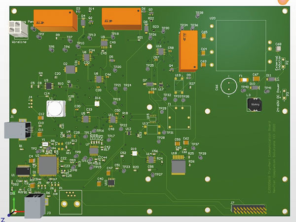
Figure 1. The original board design.
The design had four voltages: 3.3V, 5V, +15V and -15V. These were scattered across the board, and some were run using traces.
Of course, before I could update the PCB, a few minor changes needed to be made to the schematic. After making those changes, I ECO’ed the PCB. This created all sorts of issues on the PCB side. I wound up deleting all the traces and vias to help eliminate many of the issues. I then set out to update the PCB.
First, I created a PCB library for the footprints. I then added the 3-D STEP files to the footprints. I verified the footprints were accurate by comparing them to their datasheets. (I don’t trust “free” footprints.)
I then grouped the footprints – per the schematic – by voltage and purpose. Bypass capacitors were appropriately placed, as well as the microprocessor’s crystal.
One of the goals was to keep the input and output connectors in their relative locations, since this is an existing design and must fit into an existing box and connect to external wiring with minimal changes.
As I untangled the “spaghetti,” I noticed that the design began to flow, and realized that six layers were not needed. I eliminated two. Now the board was a four-layer design.
Once placement was complete, the design was reviewed. At this point, the board had a lot of extra space. The client approved a size reduction – with the proviso that the input and output connections remain in (or near) their original locations.
As such, I was able to reduce the original 8.7" x 6.5" PCB to 8.7" x 4.2" (FIGURE 2). Doing so required minor adjustments to the component placement, but I was able to accommodate the smaller PCB size with minimal issues.
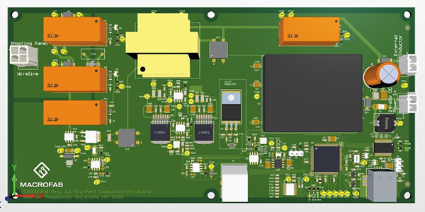
Figure 2. The redesigned board has two fewer layers and a smaller outline.
The new revision boards were fabricated and assembled. The client was able to put them into service, replacing the previous version boards. The client was very pleased with the performance, and indicated the revised design was very stable, unlike the previous version.
Disclosure: The schematic had a small issue. A few parts on the schematic were unnecessary but were not seen during the design reviews. As a solution, these parts were not assembled. Instead, a jumper was run on the board to bypass their function. If this board is respun, this will be corrected and there will probably be other functionality added, but there is no immediate need to do so. •
CID, is a senior PCB layout designer at Oztronics (oztronics-tech.com); joj@oztronics-tech.com.


Press Releases
- Adam Ryder appointed as Managing Director of Incap UK
- Metal Etch Services Opens New Motor City Facility to Meet Growing Midwest Demand
- Yamaha surface-mount line powers the future of specialized production at Inter-Company in Netherlands
- Matric Group Becomes the First U.S. Manufacturer to Deploy Panasonic NPM-GH Dual Lane SMT Technology