

A Plethora of Pitches
The unstructured evolution of integrated circuit package technology (and its consequences).
I purchased my first "integrated circuit" around 1957, which was roughly a year before Jack Kilby is credited with inventing the IC. In appearance, it was a paper phenolic PCB with six discrete transistors in TO-cans and a few axial-leaded resistors and capacitors soldered on one side. If one can stretch their thinking just a bit, however, one can see the truth of the suggestion that it was arguably an "integrated circuit." The fact that Kilby was working at Centralab in Milwaukee, a ceramic circuit maker, immediately before heading to Texas Instruments for his new job was fortuitous. I have long assumed it influenced his invention. Around the same time, the IC's recognized co-inventor, Robert Noyce, took the idea a step further and showed how transistors and interconnections could be built on silicon wafer, which remains the primary method used today – featuring sizes a few orders of magnitude smaller and significantly increased material sets to embrace many new semiconductor materials in addition to silicon.
Handling delicate pieces of silicon, was not going to "cut it," however, so IC manufacturers invented IC packages to protect the silicon chip in the assembly process. TI came up with a robust ceramic package that used microscopic gold wires to connect the I/O on the chip edges to the metal leads affixed to the ceramic, and a lid was soldered on top to protect the structure. The leads at the periphery extended straight out and were soldered to the copper metal circuits supported by a ceramic or organic base material (FIGURE 1). These were the first surface mount packages, and they flew to the moon with the crew of Apollo 11 in the navigation, control and monitoring computers on board. Another format was proposed around roughly the same time that made assembly easier, however, which was the iconic dual in-line package (FIGURE 2) invented by Bryant "Buck" Rodgers at competitor IC maker Fairchild.
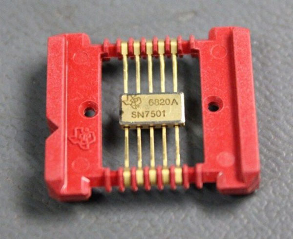
Figure 1. Many of the earliest IC packages, notably those from TI, were flat leaded and surface mounted. This carrier contains 10 ceramic ICs having 10 leads each with soldered lids.
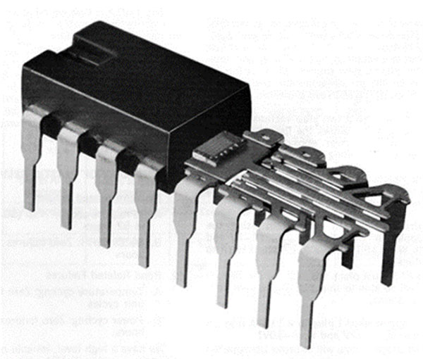
Figure 2. Structure of a DIP with die attached to metal lead frame and wire-bonded to leads to redistribute chip I/O to a standardized and more useful structure and pitch for assembly. (Source: Intel).
The DIP reigned supreme throughout the 1970s as the electronics industry exploded around the world, and the DIP format is still in use today. Among the features that made it so attractive was the pins of the lead frame carrier made hand assembly easy while being robust enough to be automatically machine inserted at high speed, plus the leads were all on 100-mil (2.54mm) centers. The former served the needs of mass assembly, and the latter eased the designing and prototyping of assemblies, with prototyping typically using "breadboards," carrier substrates fully perforated with drilled holes on 100-mil centers which could accept all common components and subsequently be interconnected using wire wrapping or direct soldering of the interconnecting wires. This technique is also still used by electronics hobbyists today to try out new ideas without having to purchase a PCB. For production, laying out a PCB on a common grid substrate could be easily done – usually without the need for a computer.
Surface Mount "Rediscovered"
The disadvantages of such "pin-in-hole" components became apparent as pin counts climbed. One was the realization that the holes required for the lead pins consumed a significant amount of printed board real estate. Another was that electrical/electronic parasitics of the long leads required to get from chip to board were significantly limiting performance in a time when PC developers were trying to squeeze greater performance from their offerings for market advantage.
In the 1980s, surface mount technology was "rediscovered." It was quickly and virtually universally recognized by the electronics industry as the answer to size, weight, cost and performance challenges faced by the industry, and a host of new components were created to address the need. First, the small outline package (SOP), then the thin small outline package (TSOP), both with leads on two sides only, followed soon after by the quad flat package (QFP) with leads on all four sides and others. With the doubling of chip transistors approximately every 24 months (in accord with the observations Intel cofounder Gordon Moore made in a 1995 update1 of his seminal 1965 paper2 projecting the trajectory of the technology) the need for more I/O and the problem of peripherally leaded components grew rapidly, thus attention shifted to area array packaging.
The advantages of area array terminations were quickly and easily understood by engineers, and the pin grid array (PGA) was quickly adopted for microprocessors because they could be socketed for testing and in use. It also allowed the user to easily upgrade to next-generation processors. Direct attachment of processors to motherboards was deemed necessary for cost and performance reasons and the ball grid array was introduced. It was beset by the challenge of inspecting the solder joint. If one cannot see a solder joint, how does one know that it is good?
The '80% Rule' Problem
Thus, peripherally leaded packages continued to be designed and used. However, to overcome the size challenge and give planners a predictive tool for future generations of products, the so-called "80% Rule" was adopted. The rule value was clearly arbitrary, resulting in "standard" I/O pitches of 2.54″, 2.5mm, 1.27″, 1.25mm, 1mm, 0.8mm, 0.65mm, 0.5mm, 0.4mm, 0.3mm, 0.25mm and 0.2mm. When one steps back and thinks over the problem of such a plethora of lead pitches, one might be reminded of the tale of "The Emperor's New Clothes." Yet the industry has held fast to the concept of the 80% rule, even though on closer inspection, the apparent absence of logical thinking has resulted in significant ongoing problems for electronics designers as each lead pitch has specific requirements in terms of solder stencil design.
The problem is also often manifested as a need to increase layer counts in PCBs to deal with the redistribution wiring required to accommodate several different lead pitches of a mix of area array and peripherally leaded components. It would have made more sense to choose a fundamental base pitch and depopulate to the desired pin count. While not a perfect solution for peripherally leaded components, it arguably makes perfect sense for area array components. This solution allows the designer to predictably lay out an assembly, reducing its size and layer count. In FIGURE 3 are shown two identical electronics assemblies designed by the same person. The first is a design completed by the designer for a work project. It was done choosing components that met functional requirements, but without concern as to the package termination, so it included a variety to area array and peripherally leaded components along with various and sundry discrete components. The second is a design completed by the same designer using the same fundamental components except that all the components are theoretically envisioned to have their I/O terminations on a common fundamental grid pitch of 0.5mm. No attempt was made to verify that all components were available with termination on such a pitch, as it was only to demonstrate the potential of using a common pitch to build what look like Lego assemblies. It illustrated the benefits that were enjoyed by the 1970s designer when 100-mil lead pitch was the de facto standard.
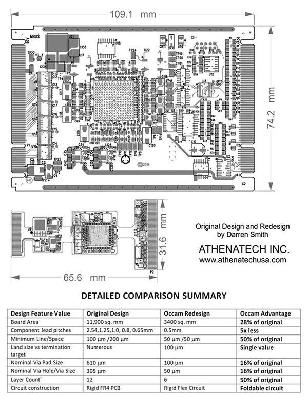
Figure 3. The comparison of designs generated by the same senior PCB designer, Darren Smith, using traditional methods versus the Occam design process, which advocates more attention to components selection (when possible). More recent thinking on the approach has suggested using packaged silicon IP blocks to allow products to be designed with the least number of transistors required.
Summary
It is evident in hindsight that the electronics industry missed opportunities to create a more coherent set of basic IC package requirements to limit the explosion of IC package types. Presently, JEDEC lists 318 registered mechanical outlines for IC packages, each with a number of lead counts and configurations. The result is thousands of choices when the fundamental requirement could well be a fraction of that number. We cannot undo the past, but we can collectively choose to use logic as a foundation for future choices to improve design efficacy and product performance and reliability.
has been active in electronics manufacturing since 1972 in various roles, including chemist, process engineer, and R&D manager. He holds nearly 190 US patents and numerous foreign ones. He is an internationally recognized expert, inventor and lecturer in the field of electronics interconnection technology and a veteran of several startup companies, including: Beta Phase, ELF Technologies, MetaRAM, Silicon Pipe, and Tessera (now Xperi). Some of Fjelstad's innovative devices and novel reliability improving IC packaging structural features are found in nearly every electronic device made today. He is also an author, coauthor or editor of several books on interconnection technology, including Flexible Circuit Technology 4th Edition, Chip Scale Packaging for Modern Electronics, and Solderless Assembly For Electronics – The SAFE Approach (the Occam Process); joseph9000@aol.com.


Press Releases
- Parmi Expands Mid-Atlantic Sales Coverage with Cope Assembly Products
- Seika Machinery to Host SMI 2026 Webinar Series Session 2 on PCB Slicing Methods and Low-Stress Separation
- Pillarhouse USA Expands BarTron, Inc. Sales Territory into Indiana
- Mycronic appoints Peter Andries as General Manager of MRSI Systems and VP of Global Technologies Division