

Closed-Loop Process Optimization between Screen Printer and SPI in an SMT Line
An experiment investigating print alignment adjustments.
Printed circuit board assembly requires extraordinary precision and repeatability. The screen printing process is considered the most critical process in the surface mount technology (SMT) assembly process. According to some studies, 70% of SMT defects can be traced back to the screen printing process (FIGURE 1). Component miniaturization has made this process more critical. Therefore, alignment of the apertures in the screen or stencil is key to an efficient and accurate solder paste transfer and there isn’t such a thing as local offset.
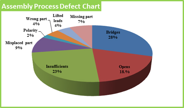
Figure 1. Solder paste defects, per Koh Young.
Every new generation of screen printers is more precise and repeatable than the previous one. External factors that cannot be controlled, however, affect the solder paste deposited on the PCBA’s solder pads. One of these factors is the stencil or board stretching. The solder brick (FIGURE 2) (e.g., the area of solder paste deposited or printed onto the printed circuit board) can be right on the solder pads in one area of the PCBA, yet off in another. It is for this reason that, sometimes, print offsets are required. This is a manual process that is performed one time. The solder paste brick could be overhanging from its solder pad if there is stencil and/or PCBA variation (stretching).
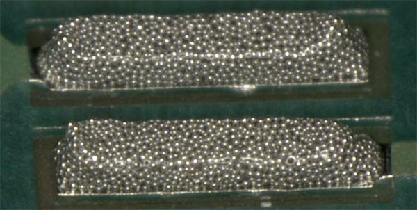
Figure 2. The solder brick.
For this reason, closed-loop systems have been developed to monitor and correct the solder paste deposition on a PCBA in real time. The closed-loop system is between the screen printer and solder paste inspection (SPI). The screen printer uses solder paste alignment information generated by the SPI to make print alignment corrections.
Stencil alignment has become extremely important due to the size and complexity of new components’ solder pads. A misalignment could compromise the gasket between the PCBA solder pad and stencil aperture, resulting in excess or insufficient solder deposition.
Screen printers have mechanisms to calculate offsets between the solder pads and stencil apertures. The methodology is limited to a few position samples, however.
The screen printer is the first process in a SMT PCBA line. To reduce the number of defects generated by this process, an SPI is placed in the line prior to the screen printer to inspect the solder paste deposition on the PCBA. The SPI measures the solder paste volume and position of the solder bricks across the entire PCBA. The results are then used by the screen printer to make print alignment adjustments (FIGURE 3).

Figure 3. How solder paste alignment improves with closed-loop feedback.
This function performs a printing position adjustment automatically, based on the SPI results. The correction values (x, y and Θ offsets) are applied to the “mask offset” of the printer program to adjust the printing position.
There are systems that require board serialization, which is another means to determine when to make the adjustments. For this test, a software counter was used to determine when to make the print alignment corrections (FIGURE 4).
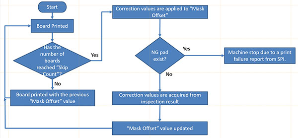
Figure 4. Closed-loop system using a counter (Skip Count).
Experimental
A closed-loop system between a screen printer and SPI machine was validated using a test vehicle (FIGURES 5 and 6).
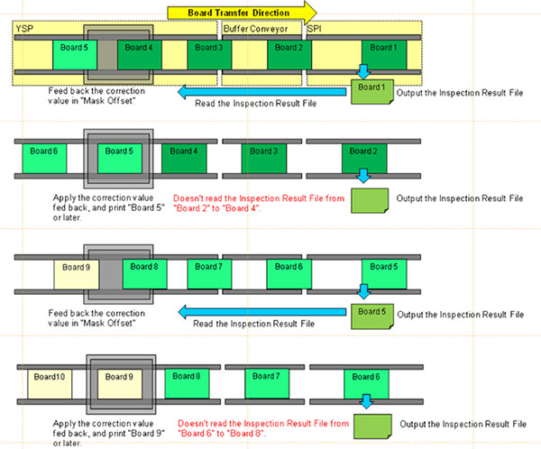
Figure 5. Diagram illustrating how closed-loop system works.
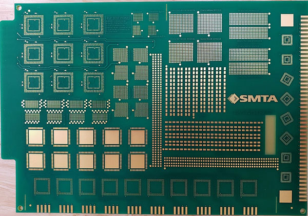
Figure 6. Test vehicle used for closed-loop validation.
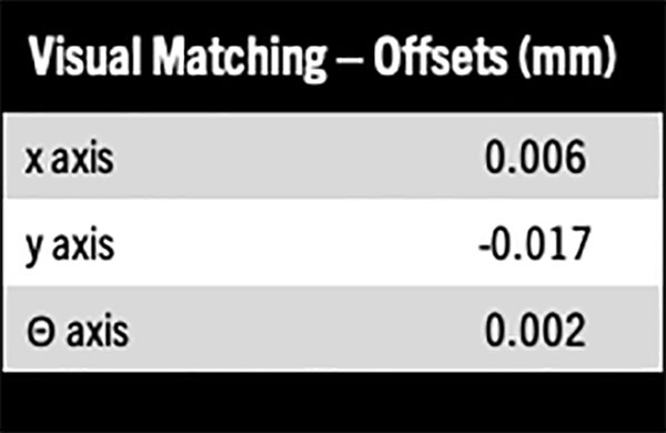
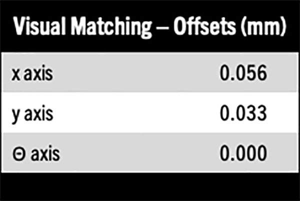
Screen printer and SPI programs were developed for this test vehicle (shown). Before beginning the experiment, the offsets between the stencil apertures and PCBA solder pads were measured using the “Visual Matching” option (TABLE 1). This option overlays solder pads with their apertures to calculate any offset due to stretching.
Table 1. Calculated Offsets Using Visual Matching
Ten PCBAs were processed through the SPI without using the closed-loop option.
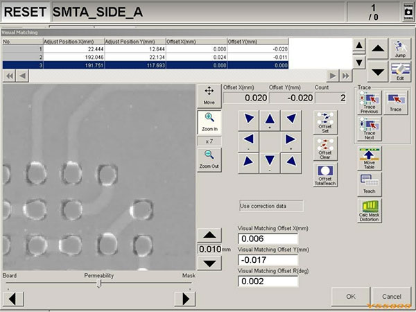
Figure 7. The Visual Matching utility used to calculate the print offset before running the PCBA.
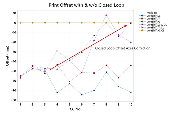
Figure 8. How the axes offset changed with and without closed-loop.
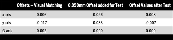
Once the print offsets using visual matching were calculated, an offset of 0.050mm in the x and y dimensions was added to the calculated offset, and the Θ axis was zeroed out (TABLE 2). The purpose was to validate that the option was working properly. All 10 PCBAs were processed without automatic stencil cleaning between prints.
Table 2. Modified Axes Offset Prior to Test
Results
The screen printer uses the SPI axes offset calculation to update its print offsets. TABLE 3 shows the final offset values after 10 prints with the closed-loop function enabled.
Table 3. Final Offset Values
We can conclude that a closed-loop system generates similar results than calculating the print offsets utilizing the printer’s utility. This utility depends on a programmer for its implementation, and it is done once. By contrast, the SPI is providing solder paste deposition offsets constantly to the screen printer when the closed-loop feature is enabled.
REFERENCES
1. Koh Young, “Why Solder Paste Inspection?” NMTronics, n.d., accessed Jul. 6, 2023, https://www.nmtronics.com/smt/koh-young.html.
2. PCBGoGo, “What is Solder Paste and How to Print It on PCBs in SMT Assembly?” accessed July 6, 2023, https://www.pcbgogo.com/Article/What_is_solder_paste_and_how_to_print_it_on_PCBs_in_SMT_assembly_.html.
is product application manager at Yamaha Motor Corp. – Robotics Division (yamaha-motor.com); miguel_colomer@yamaha-motor.com.
PCB West, Engineering Tomorrow’s Electronics
September 19-22, 2023


Press Releases
- Seika Machinery to Host SMI 2026 Webinar Series Session 2 on PCB Slicing Methods and Low-Stress Separation
- Pillarhouse USA Expands BarTron, Inc. Sales Territory into Indiana
- Mycronic appoints Peter Andries as General Manager of MRSI Systems and VP of Global Technologies Division
- The Test Connection, Inc. Becomes First Test Engineering Company in Space