

System-in-Package and Multichip Module Technology
Moving forward on the ‘More than Moore’ roadmap.
We’re witnessing a rapid evolution in advanced semiconductor nodes and market growth due to the meteoric rise of AI, mobile, autonomous automotive, IoT, communications and cloud, health tech, and wearables. The various technologies driving the overall functionality of systems and devices associated with these applications have increased exponentially, impacting factors such as device performance, energy consumption, power dissipation, and space (miniaturization).
Development of the system-on-chip (SoC), combining digital and analog, MEMS and photonic sensors, has led to the small form factors used in smartphones, health monitors, smart homes, and more. Advancements in smaller feature sizes and the resulting billions of transistors per chip translate into increased functionality, enhanced performance, and greater power – but these benefits come at a price. SoCs are hugely complex systems that generate very high NRE costs and involve other budgetary, time, and market constraints. For this reason, it has become clear that alternative technologies are now urgently needed.
The heterogeneous integration of separately manufactured components into a higher-level assembly – system-in-package (SiP) – is able to leverage the advanced capabilities of packaging technology by creating a system close to the SoC form factor but with better yield, lower overall cost, higher flexibility, and faster time to market. A recent paradigm shift from SoC-centric solutions to SiP-centric solutions has occurred, even for high-volume products.
Differences between multichip modules (MCM) and SiP technology are mainly in their respective scope and functionality. The MCM isn’t necessarily a complete system, whereas an SiP is purpose-built to be a complete system within a single package. SiP integrates multiple ICs, along with supporting passive devices, into a unified package, while the MCM represents a tightly coupled subsystem or module packaged together. An MCM can act as a cohesive unit, however, even though it may not encompass the entirety of the system’s functionality.
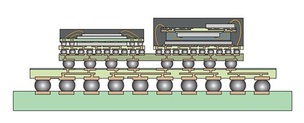
Figure 1. A SiP may contain active and passives components, MEMS, optical components, and other packages or devices, including a combination of bare dies and SMT components.
SiP, Up Close
SiP technology is a combination of multiple active electronic components of diverse functionality assembled in a single unit that performs multiple functions associated with a system or sub-system. The SiP may optionally contain passives, MEMS, optical components, and other packages or devices, including a combination of bare dies and SMT components.
SiP typically refers to standard packages (QFN, BGA, CSP, LGA) that can include different semiconductors (Si, SiGe, SiC, GaAs, GaN) and semiconductor technology generations (CMOS 65nm, 45nm, 28nm, 14nm, etc.).
The SiP-tech evolution is focused on an approach based on current and emerging generations of packages and technologies. Currently, more than 1,000 package families, with sub-groups and specialties, are available in the market. Some packages are highly specialized to niche markets, others are customized for specific functionality, while others are still more generic, serving multiple applications.
Successful design concepts will depend largely on selecting the right SiP configuration based on specific needs for each application and the availability of the components, which can then be integrated into a SiP using the appropriate technologies, including interconnect technology, die attach and seal or encapsulation technologies.
Various technologies can be used in SiP design: interconnect technologies (vertical and horizontal), encapsulation technologies (protection and stabilization), and packaging architectures. The number of available technologies for SiP implementation is growing rapidly and includes not only side-by-side integration but is also moving toward 3-D, with many different interconnect options.
Interconnect Options
Interconnection takes place a variety of ways. Vertical electrical contacts include through mold interconnection, film-assisted molding, X-via, wire stands embedded interposers, and dies. Horizontal electrical interconnects include high-density line and space using subtractive, mSAP, and SAP processes. Specific options include:
- Wire bonding, including stacking options, using various wire bonding diameters and materials.
- Flip-chip, high-resolution and high-density interconnects, enabling fan-in and fan-out technology.
- L/S high-density and high-resolution line and space, down to 25µm in substrates and 2µm in RDL technology.
- Encapsulation used to protect the sensitive wire bonds and dies from environmental influences.
- 3-D (PoP) package-on-package technology, based on a through-mold interconnect and use of a lid interconnect to enable dies to fan-out and interconnect vertically.
- Fan-out panel-level packaging (FOPLP) and fan-out wafer-level packaging (FOWLP) are among the latest packaging trends in microelectronics for higher productivity, lower costs, and higher yields.
- Interposers, which enable interconnect between low- and high-resolution substrates, matching CTE, as well as stiffening the mechanical structure (Figure 2).
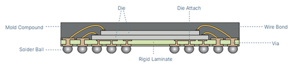
Figure 2. Cross-section of a SiP.
Applications
Most of the requirements and challenges SiP technology has faced have been dictated by the needs of the many diverse applications it serves. SiP, with all its challenges, remains a viable alternative to SoC manufacturing. Provided time-to-market and production costs remain key considerations, SiP will thrive and grow in mainstream technology.
Power functionality: Power semiconductors such as silicon carbide (SiC), gallium-nitride (GaN), and power systems in a package are becoming readily available due to innovative packaging power dissipation concepts.
MEMS functionality: Autonomous vehicles and smart homes are main drivers for sensor modules. MEMS and sensor packaging in general add many challenges to the package design picture, however, such as stress sensitivity, open access to sensor surfaces, and materials and process compatibility in sensing functionality.
Complex IoT devices/edge computing: The internet of things (IoT) can be described as a paradigm whereby objects equipped with sensors, actuators and processors can communicate with each other. IoT devices consist of a processor with an IP stack and RF interface, and require sensing abilities to interact with the ambient environment.
Application-Related Challenges
SiPs are not a panacea, of course. They come with certain challenges, including wiring density in 2-D/3-D, thermal management, COTS and bare-die co-assembly and processing, and multi-domain testing.
Functionality increases due to the growing demand for diverse device functionality means co-designing will become more relevant. Non-electronics will play a more dominant role in functionality. Co-design of non-electronic functions – optical, mechanical, cooling, and others – which were previously implemented by separate stakeholders for large systems, will now be integrated by manufacturers early in the value chain.
Assembly processes will transform challenges in SiP manufacturing – especially for multi-domain (more than Moore) functionalities, which lies in the assembly process itself – enabling next-level MCM technology (Figure 3).
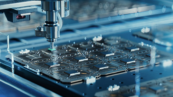
Figure 3. SiPs can be placed on panels using automated SMT equipment.
Finally, reliability requirements must be adapted seamlessly to application needs, which will bring attention to new or unaddressed reliability challenges for sectors such as automotive, aerospace and satellite.
Reliability Analysis and Testing
While significant performance, functionality and form factor improvements are enabled using advanced system-in-package and substrate technologies, a systematic approach and methodology is imperative to mitigate thermo-mechanical risk and other challenges associated with SiP solutions.
All designed package structures must be analyzed for reliability to have any application value. SiP reliability refers to the statistical probability of product failure during its lifetime, stemming from environmental effects, such as temperature, humidity and radiation, or from the application itself, such as with vibration, pressure, acceleration, etc.
While performing failure analysis for package dependability, possible issues can include warpage, chip cracking, delamination, toughness fracture, plastic deformation, and many other complications. Breaking it down further may encompass hundreds of failure items, wherein the entire analysis process becomes particularly laborious, requiring more time, higher costs and additional testing.
To keep it simple, root causes of dependability issues can be divided into three main categories: thermal management, mechanical stress and electrical properties.
Although many potential failure modes exist in system design, reliability issues mainly revolve around the following failures: stress fracture, high-temperature deformation, high-temperature deterioration, open circuit, short circuit, line impedance mismatch, electromagnetic interference, and others.
The analysis and testing of temperature, mechanical stress, and electrical system-level reliability issues are summarized below. It’s important to note that the implementation of new processes and structures can also introduce new and previously untested reliability issues. If these issues are not detected and resolved in time, they can lead to system abnormalities, causing equipment failure or even major accidents.
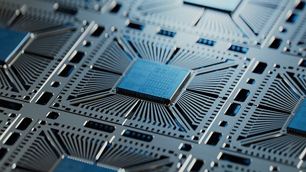
Figure 4. A mounted SiP.
Thermal management. Since no electronic device can operate at 100% conversion efficiency, as some amount of electrical energy is always lost to heat, SiP technology helps to achieve system integration with its unique advantages of small size and high density. Due to the dense placement of multiple chips, however, heat density inside the SiP is higher than that of discrete devices, with heat transfer paths further restricted by the limited space. According to the heat transfer equation, elevated temperatures caused by the SiP configuration are more pronounced than that of packages such as QFN or BGA.
Q = kA∆T/∆x
where
Q = heat
k = heat transfer coefficient
A = heat transfer area
∆T = changes in temperature, and
∆x = changes in distance.
Heat dissipation of the entire system will be impacted, resulting in elevated internal temperatures, if the thermal conductivity issues of the encapsulated system are not resolved.
Irregularities in mechanical stress become evident in cases of excessive differences in coefficient of thermal expansion (CTEs) of adjacent materials. As the temperature rises due to ongoing heat buildup, component performance is also impacted, which in turn affects the overall electrical properties of the system. As a result, most reliability issues are caused by temperature issues, which necessitate thermal simulation analysis.
Mechanical stress. Another important factor in determining the dependability of SiPs is the examination of mechanical stress. In system-level packages, materials used for chips, substrates, leads and solder connections vary. When subjected to influences such as temperature changes or other external environmental issues, various materials will shrink or expand at different rates in accordance with their unique qualities and structure. This can lead to specific consequences in deformation and mechanical stress.
To illustrate, the formula for CTE:
α = ∆l / (l × ∆T)
where
α = CTE
l = length, and
∆l = length change.
When two different materials heat up, their CTEs vary, creating a noticeably inconsistent strain on system components and resulting in extreme stress conditions. This falls under the category of mechanical stress. Loss failure and overstress failure are the two primary types of failure brought on by mechanical stress. The former refers to the buildup of low stress continuously applied over an extended period, leading to component loss (dysfunction) that produces system failure. The latter refers to failure brought on by an acute stress event or moment that far exceeds the components’ stress tolerance levels.
Much focus is placed on loss failure since such a significant portion of mechanical stress is caused by imbalances in CTE of various materials in high-heat situations. Therefore, it is imperative to investigate the specific causes of this type of failure thoroughly. Because loss failure occurs more frequently in all packing systems than overstress failure, it becomes the more valuable analysis in predicting and preventing unforeseen or uncontrollable catastrophic events.
Electrical properties – Outcome of thermal and mechanical stress. Reliability considerations with SiP ultimately manifest as problems with electrical properties because of both thermal and mechanical stress issues. Examining electrical performance is another useful technique to determine SiP dependability and to ensure that it’s functioning to specification. The electromagnetic environment of the entire package system is extremely complex. Because of the increasing density of SiPs, and interconnection channel effects on the signal, complete checks are of paramount importance. Critical factors to consider while evaluating electrical performance include EMI, SI (signal integrity) and PI (power integrity).
Conclusion
SiP is the most effective, time-to-market, cost and functionality technology available. It’s the main option able to move us forward on the “More Than Moore” roadmap.
Yaniv Maydar is vice president, R&D & Innovation at PCB Technologies; yaniv@pcb-technologies.com.


