

Identifying Solder Mask Problems with Simple Tests
Diagnosing sources of crazing, delamination and peeling.
In printed circuit board (PCB) assembly, solder mask integrity is paramount. This protective layer, designed to shield the copper surfaces and prevent solder bridging between components, plays a crucial role in ensuring the reliability and functionality of electronic devices.
Solder masks can face several issues, however: crazing, delamination, peeling, and the presence of waxy or oily residues. These defects can lead to complications like micro solder balling, bridging, and solder snail trails, especially noticeable after wave soldering processes.
Not only do these challenges compromise the PCB’s quality and long-term reliability, but they can also lead to significant production rework and increased costs.
Common Causes of Solder Mask Problems
Solder mask issues arise from several factors, ranging from the manufacturing process to the materials used. Some common causes include:
- Inadequate surface preparation. For a solder mask to adhere properly, the PCB surface must be clean and free of contaminants. Any residue or oxidation/moisture can significantly affect the mask’s adhesion.
- Incorrect curing. Solder masks require proper curing to achieve optimal adhesion and durability. Undercured solder masks are susceptible to any liquids and can be easily damaged during the soldering process due to flux absorption and improper volatilization. Insufficient hardener in the solder mask’s makeup can also cause it to never fully harden post-curing.
- Solder mask porosity. Solder masks can sometimes exhibit porosity depending on the type of solder mask used, the application process, and the curing process. Chemicals such as flux and cleaning agents as well as moisture could seep through these tiny holes. This can lead to reliability issues as well as corrosion or other damage over time.
- Environmental factors. The solder mask can absorb chemicals during PCB manufacturing, which may become highly hygroscopic or corrosive. When exposed to field conditions, these absorbed substances can cause the PCB to experience failures due to the combined effects of humidity, heat and electrical stress.
Nearly all instances of solder mask delamination are related to the PCB itself, rather than to the flux or equipment used in the assembly process. If the solder mask shows visible damage or if oily or waxy residues are present, this could indicate issues with adhesion or improper curing of the mask, or potentially a combination of factors.
Other signs of a problem include solder snail trails, micro solder balling or bridging following the soldering process. Identifying and addressing these issues is crucial to prevent compromised PCB performance and integrity.
Test Protocols
Here are a few simple tests the engineer can do on the shop floor to help zero in on the root cause.
- Adhesion check: the tape test. This test involves applying a piece of transparent adhesive tape of at least 2" in length. Press the tape on the board and pull it up quickly at an angle approximately 90° degrees to the PCB surface (Figure 1). If the tape pulls the mask off, it is a sign of an adhesion problem. The official IPC test method (IPC-TM-650, method 2.4.28) calls for 3M Brand 600 ½-inch (aka “Scotch”) tape, but if that’s not what’s in your dispenser, use whatever is.
If the mask lifts, observe the condition of the copper underneath. If the copper is shiny, it was likely not properly prepared for solder mask application. A matte finish indicates proper cleaning and roughing of the surfaces before mask application.
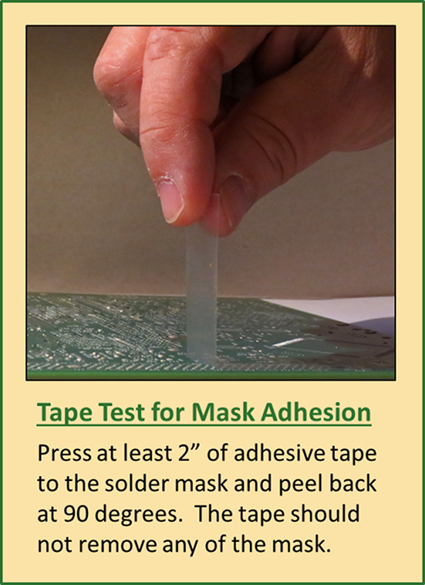
Figure 1. Tape test for solder mask adhesion.
Cure and hardness checks. Try the following three tests to check the curing and hardness of the mask.
- Pencil test. Use a freshly sharpened wooden pencil. Hold it at a 45° angle and press firmly away from you (Figure 2). If the solder mask lifts or gouges, it is not sufficiently hard. This may be the result of improper curing or insufficient hardener added to the mask before curing.
The pencil used was likely a #2H (we’re all familiar with those from standardized tests). Pencils are graded on a hardness scale, and any graphite graded less than #6H should not gouge solder mask. A #6H or a complete kit of varying hardness pencils can be found at art supply stores.
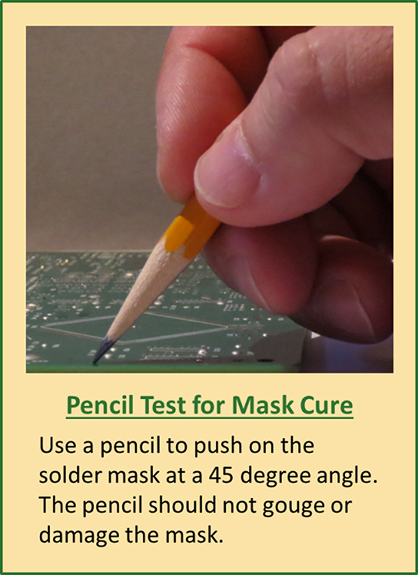
Figure 2. Pencil test for mask cure.
- Bake test. Conduct this test by placing the PCB in an oven preheated to 175°C and permit the board temperature to reach 155°C. Once at this temperature, maintain the board at 155°C for exactly 60 min. Ensure that the oven has adequate ventilation to remove any harmful fumes and plasticizers, preventing them from redepositing onto the solderable finishes, which could result in dewetting or poor wetting issues.
If issues such as crazing, delamination, and the presence of oily or waxy residues are resolved after this treatment, it indicates that the solder mask was undercured, and the additional baking has helped complete the curing process.
If the problems persist, however, this may suggest that the solder mask’s formulation was incorrect, potentially due to an insufficient amount of hardener being added during preparation.
- Solder mask check wipes. These wipes are designed for a quick qualitative test to identify undercured solder mask on PCBs. To use, remove a wipe from the package, ensuring the package is resealed. Rub the wipe on the PCB with moderate pressure for about 10-15 sec. in various areas.
If the solder mask is undercured, color from the resist will transfer onto the wipe, indicating issues with the mask’s adhesion or curing (Figure 3). If such a transfer occurs, it suggests the PCB may have defects and should be reported to the supplier for correction.
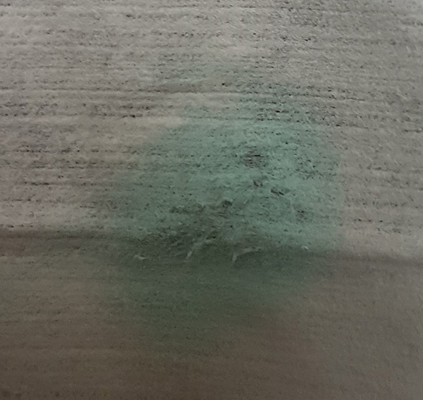
Figure 3. Greenish color deposited on a solder mask check wipe indicating a solder mask curing problem.
Case Study: How Flux Chemistry Can Exacerbate Solder Mask Issues
While solder mask problems typically stem from application issues which can be identified by the checks previously described, interaction between the mask and flux chemistry can also cause problems on rare occasions. Here we describe a situation in which the problem was at least partially flux-related.
In this case, a liquid flux seemed to be interacting with the solder mask, making it appear hazy and crazed, even lifting it from the substrate. The issue appeared to happen most frequently and severely around traces. A review of the wave solder process indicated no unusual steps, parameters, or exposure times that could cause solder mask damage, and the PCB fabricator insisted it was a flux problem.
Troubleshooting and testing. We asked the user to perform a few of the simple solder mask tests while we researched the flux lot number to determine any production changes or other customer concerns associated with it. No changes or concerns on record were found, but this particular flux was a highly specialized, small-batch material. We hypothesized that perhaps some variations could have taken place within its shelf life, so we tested a sample sent back from the user, but again found no issues.
Meanwhile, the mask failed both the tape test and solder mask wipe test. Further investigation of the mask and flux chemistries discovered that the mask was a newer, halogen-free product.
The mask’s unique composition and lack of sufficient curing caused it to remain highly porous. As a result, the flux was absorbed into the subsurface of the solder resist, where it could not properly volatilize as expected during the preheating phase.
Once the board encountered the solder wave, the absorbed flux boiled between the resist and copper layers, undermining the adhesion between the solder resist and base copper traces. This information, coupled with the solder mask test failures, helped the assembler demonstrate the problem to its PCB fabricator and drive a resolution.
It’s not unusual for the solder chemistry vendor to drive the root cause analysis of soldering issues. In fact, it makes perfect sense. The soldering technical support staff sees so many varied and different processes and problems, they are natural troubleshooters and a great resource for process engineers. Proper evaluation of material performance often relies on tests borne from the cause-and-effect knowledge gained only through experience.
is director of product management at AIM Solder (aimsolder.com); toneill@aimsolder.com.


Press Releases
- Javad EMS Upgrades Through-Hole Soldering Capacity with New SEHO PowerWave System
- Sharpen Your Selective Soldering Skills with Kurtz Ersa's July VERSAFLOW 4/55 Training
- Omron Advances Inspection Technology with NVIDIA Omniverse and Metropolis
- Seika Machinery’s SMI 2026 Webinar Series Continues with Focus on PCB Cleaning Before Solder Paste Printing