

A Comparison of Stencil Capabilities
How do modern stencil materials and coatings influence transfer efficiency and volume repeatability as SMT features continue to shrink?
The key indicators of SMT stencil performance are transfer efficiency and volume repeatability. Transfer efficiency (TE) refers to the percentage of solder paste released from the stencil when compared to the stencil’s aperture volumes and is expressed as a percentage. Typical values range from 60% to 120%.
While maximizing TE is important, minimizing variation is imperative. Variation in solder paste prints leads to rework, a non-value-added expense that risks the assembly’s functionality and reliability. Volume repeatability is expressed in terms of statistical variation. The coefficient of variation (CV or CoV) is calculated by dividing the standard deviation of print volumes by their average. It is also expressed as a percentage. Acceptable values are 10% or less. Borderline values are 10-15%. CVs over 15% are unacceptable.
Background
The relationship between stencil design and print quality is often characterized using the following terms:
- Area ratio (AR) is calculated as the area of the aperture’s PCB-side opening divided by the area of the aperture walls (Figure 1). It is an indicator of the relative adhesive forces on the solder paste deposit during separation from the stencil. As area ratios decrease, the typical percentage of paste transferred also decreases. The minimum acceptable area ratio is often considered to be 0.60 for typical SMT purposes that print with Type 4 solder paste and 0.66 when using the larger particles in Type 3 solder paste.

Figure 1. Area ratio calculation.
- Transfer efficiency (TE) is the percentage of paste that is actually transferred out of the stencil aperture onto the PCB, as opposed to what was left sticking inside the aperture walls or on the bottom of the stencil (Figure 2). It is calculated as the average paste deposit volume divided by the aperture’s volume and expressed as a percentage. A common benchmark is 80% TE.
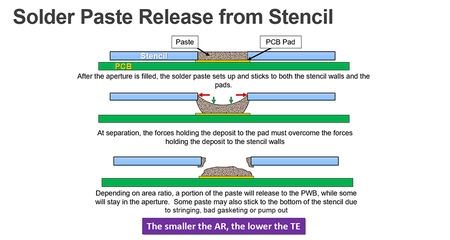
Figure 2. Opposing forces in solder paste release from stencil aperture.
TE is often plotted as a function of AR to characterize stencil release. Figure 3 shows a typical TE plot for different stencil types, and Figure 4 shows actual photographs of release for different Ars.

Figure 3. Typical TEs of different stencil types.

Figure 4. Side-view photos of paste deposits at different ARs.
ARs and TEs may be either theoretical or actual. Theoretical ARs and TEs are calculated from the stencil specification, whereas actual ARs and TEs are based on actual measurements. The TEs reported by solder paste inspection (SPI) machines are theoretical, based on the apertures’ CAD dimensions and thickness.
Variation. Minimizing variation is critical in fine feature printing. Print volume variation can lead to opens, shorts, head-in-pillow and tilted component defects. High variation indicates an out-of-control process that may be creating both obvious and hidden defects.
Cpk, or the process capability index, is a popular and common metric for indicating manufacturing variation. It is usually calculated using a target or goal of 100% volume and upper and lower control limits of +/-50%. In cases involving solder paste volumes, where average TEs are often below 100%, standard Cpk calculations can skew the metric unfavorably.
Example: If the average solder paste deposit is 200 cubic mils and the standard deviation is 20 cubic mils. CV = 20/200 × 100 = 10%
If the average deposit is smaller – say 50 cubic mils – but the standard deviation is still 20 cubic mils.
CV = 20/50 × 100 = 40%
Both cases have the same absolute spread, but the smaller deposit is much less consistent relative to its size. This is why CV is more meaningful than standard deviation alone.

Figure 5. Modeled Gaussian curves show the impact of CV on solder paste volume consistency.

Figure 6. Relationship between CV and control limits.
Interpreting CV in Solder Paste Printing
- CV <10% stable and desirable: A CV below 10% indicates a very stable process. Statistically, 99.7% of solder deposits will fall within ±30% of the average volume. For example, if the average deposit is 200 cubic mils, nearly all deposits will land between 140 and 260 cubic mils. This is well inside the typical process control limits of ±50%.
- CV ≈ 15% borderline / at risk: At around 15%, the variation grows. Here, 99.7% of deposits fall within ±45% of the mean. For a 200 cubic mil target, that means deposits ranging from 110 and 290 cubic mils. While still technically within process limits, the margin is tight. Any drift in stencil condition, paste rheology, or printer setup could push the process out of control.
- CV > 16.7% out of control: A CV above 16.7% signals excessive variation and an unstable process. Too many deposits will exceed the ±50% control window, leading directly to defects such as opens, insufficiencies, bridging or head-in-pillow failures.
The CV measures the repeatability of solder paste deposits relative to their mean size, providing insight into process stability. While high TE confirms that sufficient solder paste is being deposited, low CV demonstrates that the deposits are applied consistently across the board. Together, TE and CV form the foundation of a reliable solder paste printing process, ensuring consistent joint formation and long-term assembly reliability.
Experimental Methods
Print tests. The top side of the SMTA miniaturization test vehicle is shown in Figure 7. The top side was printed. Clean, new boards were used for the tests.

Figure 7. A SMTA miniaturization test vehicle.
All stencils were print–tested simultaneously on the same run, using the same setup, paste and SPI machine (Figure 8).

Figure 8. A printer and SPI machine in the laboratory.
The typical 10-print test was used for all stencils. The 10-print test consists of two knead strokes, a dry underwipe and 10 consecutive prints with a dry wipe between each print. The first print is always back-to-front to visually ensure the paste is rolling properly.
Printed boards were then automatically passed via conveyor to the SPI. Print tests took place at the Parmi demonstration laboratory in Hopkinton, MA, using the following equipment and materials:
- Printer: ITW MPM Momentum
- SPI: Parmi Sigma X certified by CeTaQ3
- ScanCAD stencil inspection equipment
- Paste: Indium 8.9 HF Type 4
- Squeegees: 60-degree Surgical SS with backing plate
- Six stencils from three different suppliers; one uncoated and five with nanocoating
- Standard underwipe textile, no solvent used
To aid in debugging print results, stencil measurement software was used to scan the stencils and compare the aperture openings to their theoretical sizes. The system uses a high-resolution scanner to capture the stencil image and software to overlay CAD designs and compare actual aperture sizes with their designed dimensions.4
Data Analysis Methods
Datasets for the 0201, 05BGA, 04BGA and 01005s are exported to a comma-delimited file. Each dataset contains the
- Measured volume (mils)
- Theoretical transfer efficiency, TE (%)
- Actual area measured at the 20µm threshold
- Theoretical area % at 20µm threshold
- X offset* (mils)
- Y offset* (mils)
- Panel index**
- Time stamp.**
* Offsets are not used in calculations for these tests but are always exported to help in diagnosing seemingly anomalous data, such as excessive volumes due to aperture-pad misalignment.
** Panel ID and time stamps are recorded for purposes of clarification when reviewing data.
The datasets are then imported into an Excel spreadsheet. Several different analysis methods are applied. Pivot tables are used to calculate the average and standard deviation of the measured solder paste volumes. The CV is then calculated and analyzed. Data with CVs indicate the edge of the process window, where slight input differences can have considerable effects on process outputs.
Experimental Results
Initial results showed similar TEs for most stencils, but one stencil showed far superior performance – so superior that it was suspicious (Figure 9). An investigation subsequently revealed that the wrong stencil design was used. The data were excluded from the analysis; however, the investigative methods and results are reviewed.

Figure 9. SPI TE results.
Table 1 shows TE and CV results for the remaining five stencils. The 0.5mm BGA (05BGA) exhibited an interesting range of CVs in or near the 10-15% range. Therefore, the solder paste volume and release data for the 05BGAs are the focus of the analysis.
Table 1. Chart on TE Results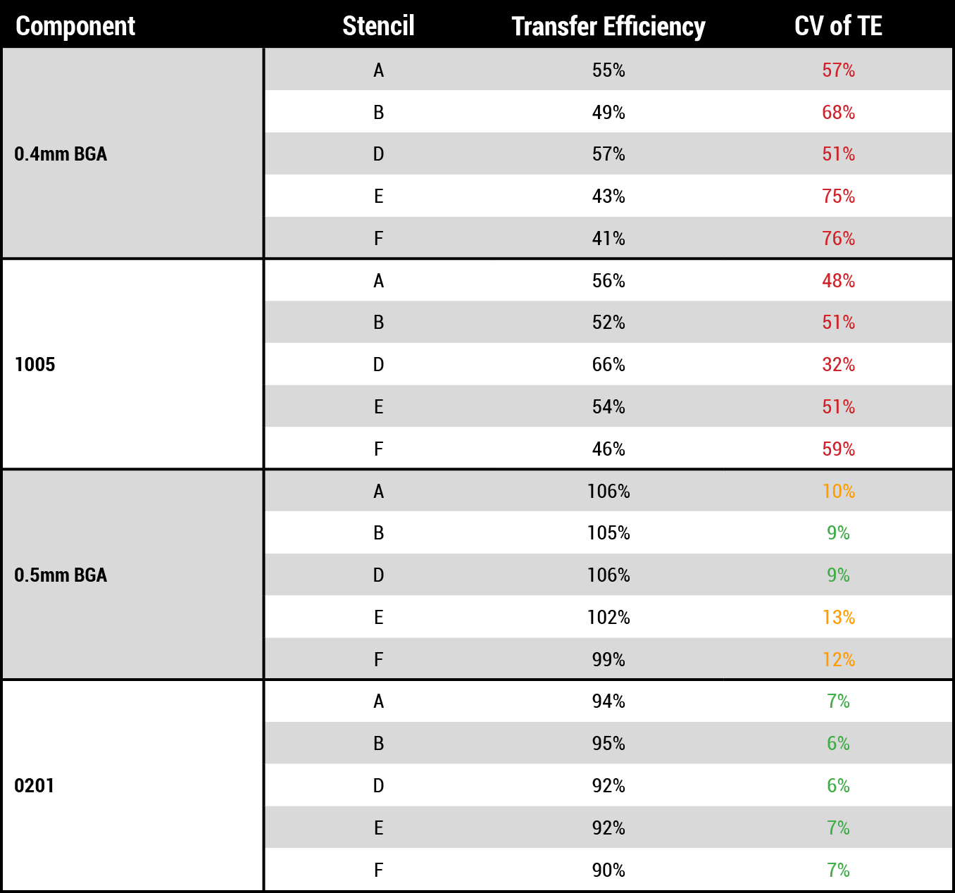
Print data from the 10-print test may be analyzed in multiple ways. First is a simple run chart showing the volume of each print (Figure 10). The average volume shift between prints indicates uniformity across back-to-front and front-to-back strokes and the “leading edge” effect. In this experiment, average volumes ranged from approximately 360 to 420 cubic mils across stroke directions, with greater variability in earlier print strokes than in later ones. The stroke-to-stroke variation may be partially attributable to machine calibration and partially to the leading-edge effect of the PCB design.

Figure 10. Average volumes of 05BGAs for prints 1-10.
Of particular interest is Stencil A, which was obviously run in opposite squeegee directions from the rest of the stencils tested.
Run charts often show that paste volume increases and variation decreases in the first few prints as the paste reaches its working viscosity from rolling on the stencil. Note that two knead strokes were applied before the first print to begin shearing the paste down to lower its viscosity.
The histograms in Figure 11 show the distribution of the data. Taller, narrower bell curves are preferred over shorter, wider bell curves, because they show a tighter distribution. Their tighter distribution indicates better process control, less obvious defects and rework, and less latent joint failures in service.

Figure 11. Histograms showing the distribution of data.
Review of the histograms: notice that the means are not 100%, indicating the use of CV over Cpk as a metric of paste volume repeatability. A Cpk metric would be skewed by calculating Cpk based on 100%, +/-50%, because the process would not be considered centered in the window. Also, notice that Stencil E has a relatively large CV due to its many insufficient solder deposits. Based on histogram analysis, Stencil D provided the tightest distribution of print volumes.
Box and whisker plots also show the average volume and spread of the data, but offer more interesting insights. In a boxplot, the data set is divided into quartiles (Figure 12). The box represents the middle two quartiles (Q2 and Q3) of the data. The average or mean – represented by the X – may or may not be in the middle of the box. The whiskers represent the outer two quartiles (Q1 and Q4), indicating the overall spread of the data. Outliers are calculated statistically.

Figure 12. Boxplots of 05BGA volumes from different stencils.
Outliers are important in reviewing SPI data. Outliers above the upper whisker indicate excessive volumes, which are often due to gasketing issues, and are less worrisome than insufficient volumes. Outliers below the lower whisker are more prevalent on fine feature prints and can result in fragile solder joints. The frequency of insufficients and zero volume reading are more visible in box and whisker plots than histograms or CV calculations.
Review of the b and whisker plots shows that Stencil D has the tightest distribution, but Stencil A has fewer outliers, particularly on the more dangerous lower end of the spectrum.
Zero volume readings in SPI. On fine-feature prints, the SPI may read and report zero volume, despite visible paste on the pad. SPI machines read solder paste deposit volumes at a height threshold off the board; typically, that Z-height is 40µm above the board surface. The algorithm precisely measures the solder paste volume above the threshold and calculates the volume under the threshold by multiplying the area at the threshold by its Z-height. Solder paste that does not cross the threshold does not get included in the measurement or calculation. In this test, the threshold was set to 20µm.
Discussion of Results
All five stencils performed respectably. One stencil was not coated; the others were coated with very thin nanocoatings. These coatings lower surface energy to enable better release, but they do not always compensate for aperture wall roughness (Figure 13).

Figure 13. High magnification views of stencil aperture walls.5
Previous studies have indicated that thinner fluxophobic coatings reduce variation by approximately 25%, whereas the thicker, spray-coated and cured coatings reduce variation by as much as 50%.
It has been hypothesized that the reason the thicker coatings provide lower variation is that they fill in the small fissures in the aperture walls created by the laser-cutting process. The reduction in wall roughness essentially lowers the surface area of the aperture, positively affecting its actual AR and improving the boundary condition of the paste-aperture interface by leaving fewer places for solder particles to bind when flowing through the stencil.
Thicker polymer coatings have also demonstrated quantifiable TE benefits at ARs as low as 0.50. But because of the coatings’ physical thickness, they may become self-limiting in the future as aperture sizes continue to shrink. Thinner coatings will ultimately be needed to extract the benefits of nanocoating in future miniaturized electronic assembly processes.
All the stencils tested showed good process capability for 0.5mm BGAs with ARs of 0.63, but poorer capability for 01005s with ARs of 0.50. These results are typical for Type 4 solder paste with 4 mil stencil thickness and ultrathin nanocoatings.
Stencil Discrepancy Investigation
Several avenues were pursued to understand why Stencil C printed so differently from the other five.
The first step when investigating high solder paste volumes is to review the X and Y offsets. Poor gasketing is often the root cause of excessive solder volumes. As shown in Table 2, most X and Y offsets were less than 1 mil, thereby excluding them as possible root causes of excessive deposit volumes.
Table 2. Average Print Offsets
The next step was to review areas with excessive pressure, indicating possible “pump out” or “squeeze out” from high pressure that disrupts gasketing or stringing due to release issues.
Table 3 shows the average area % readings for each stencil. The disproportionately large areas of Stencil C on three of the four device types supported the hypothesis that something was different in C’s dataset.
Table 3. Average Print Areas
The third avenue was to examine the potential for experimental execution errors. The original data was re-exported and re-analyzed. The numbers were identical, eliminating data transfer as a root cause.
The stencil was then reprinted using the same solder paste. The data correlated with the first test’s results, indicating no errors in setup or execution.
The stencil was then visually reviewed, but no discrepancies in the apertures in question were noticed.
The stencils were sent out for scanning to measure the apertures. The scanned and compared images revealed the differences. In the close-up view of the scanning results (Figure 14), the actual aperture is round, whereas the aperture design is a squircle – a square with rounded corners.

Figure 14. ScanCAD image of actual stencil vs. Gerber data.
The shape of the apertures was not exactly the same as the CAD, but they were not very different, and therefore, not easy to discern. Other apertures on the stencil overlay were recognized from a previous experiment, and the Gerber files were still available for comparison.
In the test stencil design, the 04 BGAs and discretes had smaller apertures than the ones on stencil C. The default stencil design for the 04BGAs is a 7.5 mil squircle; Stencil C had an 8.5 mil circle. Figure 15 shows the overlay of the two and the impact on area ratio.

Figure 15. Shape, size and AR differences in CAD.
The default stencil design for the 05BGA device is a 10 mil squircle; Stencil C had a 10.8 mil circle. Of the four aperture designs studied, the 05BGAs were the most similar in geometry. Referring back to Figure 8 and Table 3, these apertures produced the closest volumes to the default stencil design. Because the designs were not exact, and Stencil C had an AR advantage, the data remained excluded from the analysis.
Conclusion and Discussion
Solder paste print processes with CVs below 10% are considered very stable. Print processes with CVs greater than 17% are considered unstable and out of control by standard criteria. Processes with CVs in the 10-15% range offer excellent opportunities to understand the edges of the process window.
In this study, the 0.5mm BGAs produced CVs within the typical range for the test process used. Therefore, the dataset for the 05BGAs was selected for further analysis.
The five stencils with the same aperture designs performed as anticipated. Stencils A through D and F were coated with different coatings; stencil E was uncoated. It had the largest CV, the widest distribution, and the most insufficient deposits. All coatings outperformed the uncoated stencil.
A key takeaway is that all four coatings outperformed no coating. While some combinations of metals, laser-cutting technologies, and nanocoatings may exhibit performance advantages over others, one fact remains consistent: nanocoating is better than no coating, every time.
Multiple methods of evaluating stencil and printer performance were introduced and reviewed, including:
- Run charts help illustrate the differences between front and rear print strokes, as well as the number of strokes for the paste to reach its working viscosity.
- Histograms show the spread of the data. In the context of solder paste transfer, they are rarely centered at 100%.
- Boxplots also show the spread of the data but make outliers more visible than histograms.
- Pivot tables enable fast and easy data manipulation, including basic statistics on volumes, TEs, areas and offsets for analysis.
Statistical analysis software can yield more sophisticated insights into the main effects and interactions of input factors than spreadsheet-based analysis, particularly when additional factors are introduced. Spreadsheet analysis is fast, easy and accessible, and pivot tables provide excellent opportunities to run “what if” scenarios and identify trends, however.
Lessons Learned
In addition to the planned results from this study, three valuable learnings were also realized:
- If data looks anomalous, do not ignore them. Investigating spurious data may lead to new discoveries or, in this case, cleaner data. Had this dataset been part of a multivariable DoE analyzed without human review, the aperture discrepancy would have grossly skewed the main effects and interactions results – and perhaps the conclusions and subsequent critical decisions.
- Always use SPI to verify a stencil before a run. Using the two-print test shown in Figure 16 would have immediately indicated the differences in Stencil C.
- Cut test coupons similar to those shown in Figure 16 in the corners of the stencil for ease of measurement. This practice has been recommended since 2014, but was not followed in this experiment. It will be reintegrated into the next revision of the SMTA Miniaturization Test Vehicle (MTV) stencil artwork.

Figure 16. SPI stencil verification flow chart.
Recommendations and Future Work
The quest for electronics miniaturization will never end. Manufacturing processes will continue to develop in order to support the ongoing trends.
As feature sizes shrink with the advent of ultra high-density interconnect (UHDI) technology, the solder paste deposition process will address new challenges with more evolution:
- More accurate and repeatable deposition hardware
- Thinner, stronger stencil foils
- Types 5 and 6 solder pastes
- More advanced test vehicles.

Figure 17. Test coupons for measuring stencil apertures.
The “original” SMTA test vehicle, designed in 2017, was used for this test because it has a long history and a very large database, which can be used to compare print performance. Even this MTV test board faces impending obsolescence as it gets phased out in favor of a more contemporary, 2025 version referred to as the UHDI board (Figure 17).
References
- C. Shea, “Stencil Printing – Advanced Topic,” webinar, SMTA Knowledgebase. https://smta.org/page/knowledge-search#archived-webinars/entry-details2/5e8d4965f6f94c06c598442b/
- D. Dixon, et al. “Development of a Solder Paste Test Vehicle for Miniaturized Surface Mount Technology,” Proceedings of IPC Apex Expo, 2018.
- CeTaQ, Independent Machine Capability Analysis Services, company website, https://www.cetaq.com.
- ScanCAD International, Advanced Imaging and Software Solutions, company website, https://scancad.net.
- C. Shea, “Advanced Topics in Stencil Printing,” professional development course, SMTA International, 2019.
Acknowledgments
Many thanks to Travis Loving of ScanCAD and Doug Dixon of 360Circuits.com for their support in solving the mystery of the spurious data.
Ed: This article is adapted from a paper first published in the Proceedings of SMTA International 2025, and is reproduced here with permission of the authors.
is owner at Shea Engineering Services LLC (sheaengineering.com), and a four-time recipient of the SMTA International “Best of Conference” award. is application engineer and is application manager at Parmi (parmi.com); atorres@parmiusa.com.


