

Finetech Releases Femto 2 Bonder
Femto 2 die bonder, for advanced packaging and bonding, has a placement accuracy of ± 0.5µm @ 3 Sigma.
Supports a range of applications at chip and wafer level. Is suitable for optoelectronics, semiconductors, silicon photonics, medical engineering, sensor production and R&D. Supported applications include laser diodes, laser bars, VCSEL/PD, LED packaging, active optical cables (AOC), optical engines, TOSA/ROSA, lens attach, MCM, MEMS, sensors, WLP, 3D IC / 2.5D IC, TSV, C2C, C2W, chip-on-substrate, chip-on-glass, chip-on-flex, and more. 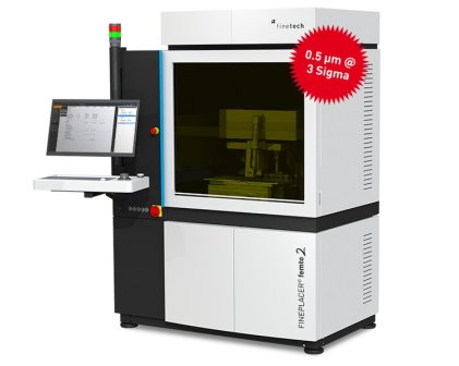 Configurable for specific applications with a range of process modules, enabling many bonding technologies: eutectic and epoxy die attach, adhesive bonding and curing, thermo-compression bonding (force from 0.05N up to 1000N) and thermo-sonic bonding, diffusion bonding (SLID, TLPB, Cu-Cu), as well as laser-assisted die bonding, bump bonding and copper pillar bonding - on a single platform. High-quality dispensing options allow lines, dots and patterns, as well as micro dipping solutions for smallest components and contact areas. New vision alignment system is designed for very high precision requirements and provides uniformly sharp representation of finest structures across the entire field of view. High-speed heating plate provides ramps >60 K/s for reproducible heating, ramping up and down without overshooting.
Finetech, www.finetechusa.com


Press Releases
- ViTrox Americas Welcomes Doug Ennis as Senior Field Applications & Service Engineer
- Altus Adds LPKF CuttingMaster 3290 to Depaneling Portfolio
- Kurtz Ersa Partners with E-tronix for Sales in Illinois and Wisconsin
- XLR8 EMS Welcomes Raul Jorge Lopez Jr. as Director of Program Management and Procurement