

What's Old is New
To close the gap in IC substrates, buyers need skin in the game.
 The CHIPS Act was passed more than a year ago and not one federal dollar has yet to be awarded – although private industry has committed and started to spend billions. Once funded, the new, more advanced foundries will take years to build and start operations.
When produced, however, the chips will be useless until they are packaged and mounted on PCB platforms. The facilities, materials and knowhow to produce the substrates used to package them remain primarily in Asia – including China.
Notably, the cost to build and equip the necessary substrate and PCB facilities to produce HDI and UHDI (ultra-HDI) circuitry in volume is substantially more than that of a typical PCB or flex circuit factory, but far less than that needed for a foundry.
To provide incentives, US Representatives Blake Moore (R-UT) and Anna Eshoo (D-CA) this year introduced H.R.3249 – Protecting Circuit Boards and Substrates Act. This bill is the second iteration of this effort and has a long way to go in gaining cosponsors and approval.
Creating sustainable Western PCB and substrate sources will take time, and will not necessarily be in the country of use. Today just a handful of American and Western companies have the technology to produce some level of UHDI circuitry. To develop a secure source, the US will need more than government words, resolutions, bills and funds with heavy ropes (not just strings) attached: It needs active OEM investment and participation.
The PCB East keynoter gives a roundup of innovative technologies to come out of the pandemic.
We have gone where no mask has gone before! The Printed Circuit Engineering Association (PCEA) held its first regional conference and exhibition in Marlborough, MA, in April.
A resurrected PCB East drew attendees from as far as the West Coast and Florida. There is nothing like in-person contact. The social aspect of networking has been missing for far too long. The enthusiasm of the attendees bodes well for future face-to-face regional gatherings.
It was great to see so many old friends in the real world, while meeting new young engineers and entrepreneurs such as Yitzi Ehrenberg and David Kanarfogel of Conformant, who have developed a new additive circuit process based on an innovative CVD system.
IPC and retired industry legend Dr. Laura Turbini joined many notable attendees, including Dr. Hayao Nakahara, Anaya Vardya, John Vaughan, Chrys Shea and Peter Bigelow, president of the SMTA Boston Chapter.
The many design and engineering programs conducted during the three-day meeting and exhibition by such experts as Susy Webb, Rick Hartley and Steph Chavez brought attendees up to date.
In step with the expanding revolution of 3-D printing offering the ability to create previously unimaginable structures by the precision dispensing of a variety of conducting and insulating materials, Dr. Jaim Nulman of the AME Academy stirred our imaginations with a two-hour introduction to 3-D additive manufactured electronics.
During my keynote “From Possibility to Reality,” I discussed new and emerging technologies from Israel, Germany, the US and Japan. The image of a rocket spike created by Hyperganics’ algorithmic engineering platform that used AI to design and print the complex part amazed a full lecture hall. The detailed combustion chambers, which can only be created by software, ensure it doesn’t overheat.
The theme was Covid Class Creations: products and processes developed, improved, modified and introduced during the pandemic. A number of new products under advanced development or on the verge of commercialization not yet seen in the marketplace were presented.
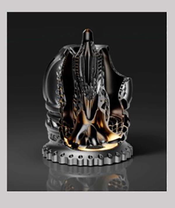
This aerospike rocket engine was engineered in Hyperganic Core using advanced software algorithms and has never seen a single piece of manual CAD. It’s likely the most complex additive manufactured part ever produced; it broke all conventional workflows. The part could not previously be designed, let alone built. It is said to be about 20% more efficient than previous bell-shaped parts.
Luminovo’s rapidly growing software suite for PCB design and manufacture, not yet available in the US, drew a lot of attention. Among its features is one that can calculate and predict design violations. It also calculates supply chain risk assessments.
Averatek’s A-SAP process (semi-subtractive process, or SSP, by some) allows the design and fabrication of 25µm lines and spaces, illustrated by a part produced at American Standard Circuits, as was Rogers’ new resin for 3-D additive manufacturing (by spray) that resulted in printable and plateable parts.
Atotech’s new electroless – yes, I said electroless, not immersion – tin process was intriguing! The process did not dissolve copper from the base plated, is not dependent on its position in the periodic table in reference to the metal(s) – usually copper – and did not stop depositing when the base was sealed. Therefore, no dissolved copper contaminates the solution. The company also introduced a new oxide replacement for MLB manufacture, which left a smoother surface for HF and VHF needs.
As we contemplate new materials for 5G and 6G applications, Isola introduced hybrid laminates, combining PPE with outer layers on FR-4, as well as other combinations. The company also provided data on its new green materials.
Nano Dimension provided information on the progress of its activities to make 3-D ink-jetted printed circuit structures containing passive components, 75µm lines and spaces, and 45° pad-less interconnects between levels with its most recent DragonFly IV system.
PulseForge’s use of photonics to replace IR or laser for soldering permits soldering to curved or flexible surfaces, soldering to PET or paper (e.g., LEDs to flexible substrates), reel-to-reel and soldering batteries to substrates for single-use medical devices. The use of photonics can be used to cure protective coatings or sinter metallic pastes – all in seconds with 75% less power than IR. The company illustrated its activities to develop cycles for BGA assembly. The photonic soldering process reportedly provides fewer voids in SAC alloy joints than conventional thermal processes.
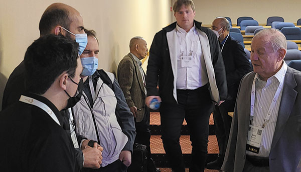
The author (right) greets attendees following his keynote at PCB East in April.
IO-Tech, winner of recent innovation awards at Productronica and Lopec, introduced its unique patented laser system for application of precisely and rapidly depositing type 6 solder spots with resolution of 100µm in diameter and 25µm (or finer) pitch – faster than dispensing 2,000 droplets. I predict fabricators will be challenged to make substrates that take full advantage of this system’s capabilities! Die bonding is another potential application for this system, as deposits are extremely flat. (Roughness is <5µm.) It can print on components for multiple chip stack applications. And, for this application, the system is said to be faster than dispensing 10,000 droplets.
This is only the beginning of a new age in the design and manufacture of electronic packages. It’s difficult to see how the chip shortage problem will be resolved in the near future, as the world’s supply chains are experiencing new disruptions due to the conflicts in Europe. It is also too soon to know how or if active components will be part of the future of additively built constructions.
In the interim, we’ll continue to see more consolidation. There will be more vertical integration. Partnering and cooperation, perhaps even system or facility sharing, will increase.
Even when supply chain issues are resolved, we still need to build new infrastructures for the new designs promulgated by so many new innovations. Then we will need new standards and new tests to determine quality.
Stay tuned! Better yet, join the parade and march forward with your contributions to the developing world of electronic design, manufacture and packaging.
is a business and technical consultant dba Weiner International Associates, serving the specialty chemical and electronics industries. His clients have included several Fortune 100 companies. His executive experience includes president of New England Laminates; vice president of sales and marketing of Dynachem, and director at Wong’s Kong King International; gene@weiner-intl.com.
How prepared is your organization?
Here we are in January 2022 with a future fraught with more uncertainties than any other during my six decades in the PCB, IC fabrication and assembly industries.
Business is strong despite shortages in labor and parts. Prices are rising, dramatically in some cases. Profits are being squeezed. Rapid government changes in travel restrictions and worker conditions seem endless due to the continuing evolution of the pandemic.
Supply chains are under pressure from a variety of events and circumstances. These include some brief power shutdowns at plants that produce wafers and PCBs in China, chip and other component shortages, shipping issues with a backlog of over 100 cargo ships carrying, for example, container loads of copper-clad laminates anchored off the Southern California coast waiting to be unloaded. The battery industry is gobbling up copper supplies. Major consumers are buying into chipmakers who can guarantee their needs. This affects those who cannot, causing them to scramble for new sources.
Not only are ICs in short supply, especially for automotive needs with the increase in the manufacture of EVs and hybrids, but substrates are needed for their mounting and connection to the outside world. As a result, major automotive companies in Japan, the US, and Europe have curtailed production in several factories to the tune of several million vehicles in the coming year.

Press Releases
- RBB Welcomes Shawn Myers as Engineering Project Manager
- ECIA’s Market Sentiment Index Average Hits Five-Year High in June Industry Pulse Survey
- Incap Slovakia invests in cleanroom capability to support semiconductor manufacturing requirements
- Orbit Technologies accelerates growth and doubles production capacity with Europlacer iineo placement machine