Current Issue
How and Why to Use the IPC-9641 Standard
The new PCB flatness guidelines cover machine selection, measuring and testing, to which our author adds some best practices.
Foreword
In late 2011 there was a growing concern that the PCB industry was not keeping in step with component substrates' need for flatter boards at elevated assembly reflow temperatures. This situation was showing up as lower assembly yields and higher rework for some components. The need to understand how the board reacts during assembly reflow was not being met by the existing IPC-TM-650 Method 2.4.22, Bow and Twist. JEDEC had publications for components in place that set flatness requirements at elevated temperature but there were no corresponding publications for the board. This growing concern led a group of OEMs, EMS, PCB fabricators and measurement equipment suppliers to form the IPC 6-11 Printed Board Coplanarity Subcommittee in early 2012. The time was right for a new look at board flatness and the committee developed and passed the IPC-9641 High Temperature Printed Board Flatness Guideline within a year from its’ inception. IPC-9641 is a guideline and as such, was developed to provide a standardize methodology for evaluating board flatness at elevated temperatures so that the electronic industry can have meaningful discussion on the interaction between component and board at this critical time in the assembly process. It is the committee’s hope that the PCB industry will start to collect the elevated temperature data on its products prior to setting any limits or specifications. These data will help OEM and PCB designers gain some fundamental knowledge of board movement and be prepared for any future board flatness requirements.
IPC-9641, High Temperature Printed Board Flatness Guideline, has been approved and released by IPC. For the first time, an international standards organization addresses local area PCB warpage across reflow profile temperatures. The standard provides guidelines for selecting measurement equipment, planning testing, preparing PCBs for test, performing measurements across reflow temperatures, and reporting local area warpage results.
Measuring and controlling package warpage across the full thermal reflow profile has been standard practice for years and is seen as critically important to final product yield. IPC-9641 has been approved because IPC members have determined that, as stated in the introduction to the standard, “… controlling the board flatness is equally important for preventing subsequent assembly-related issues, including open or bridging joints, which ultimately cause product failure.” Assembly-related issues also include challenging problems such as head-in-pillow that ultimately lead to field failures and product returns. So, while for many years the package was held up for scrutiny as the only relevant contributor to warpage-related assembly defects, now the other side of the attach interface, the PCB land area, has also been identified as a potential contributor to defective assemblies. It’s now important to understand, quantify and control the warpage of PCB areas where packages attach across temperatures.
The standard is both educational about the general topic of PCB warpage measurement and specific in its guidelines for how such measurement should be done. The standard provides a starting point and a point of reference as companies begin to build, or to improve, PCB warpage measurement systems. As an additional benefit, when dynamic warpage information is obtained from PCB areas, these data can be shared with those responsible for package manufacturing and SMT assembly to facilitate continuous improvement in both component shape compatibility and final product quality.
The rest of this article consists of a summary of the contents of IPC-9641, followed by some notes about how to implement it using practical best practices derived from years of measuring packages and PCBs.
Section 1 – Purpose. A concise statement of the purpose of IPC-9641 comes from its introduction: “This document aims to provide guidance on methods and procedures for critically evaluating printed board flatness during a simulated temperature reflow cycle.”
This section introduces the intent of the standard, explains its scope and how it differs from existing standards, and includes a glossary of terms that are defined to provide a common understanding of meanings of the warpage-related technical terminology that appears later in the document. It also lists other documents and standards (such as Jedec JESD22-B112) that preceded this one and can provide appropriate historical context. For those involved with warpage measurement, the glossary may serve as a useful reminder, and for those not yet measuring warpage of any type, it may serve as an invaluable reference.
Section 2 – Applicable documents. This section is simply a list of all related Jedec, IPC, and Joint Industry Standards, for serious students of the subject who want to review all available publications from these bodies that provide context for IPC-9641.
JESD22-B112, High Temperature Package Warpage Measurement Methodology, is the most closely related standard on the list. It details a method for consistently measuring package warpage, like IPC-9641 addresses measuring the corresponding land areas on PCBs.
Section 3 – Measurement instrument requirements. This section reviews different metrology technologies and the theory behind how they work. It is the most purely “educational” section of the document, and explains shadow moiré, projection moiré, fringe projection, confocal and optical coordinate measurement technologies. These are the metrology methods for PCB local area warpage measurement “recommended” in the standard. (Each technology is only briefly discussed, and pros and cons or tradeoffs for each technology are not fully addressed, so this section is best used as an introduction to the topic of potential measurement technologies, and supplemental research would be prudent.)
Section 4 – Parameters of interest. This section lists contributors to PCB warpage, including design and manufacturing variables. It notes that it is easier to change the manufacturing parameters than the board design itself.
The effects of clamping and board support methods are explored. Diagrams and static equations illustrate the mechanical effects of constraining the PCB during reflow assembly. The purpose of this section is to emphasize the importance of mechanical support and clamping constraints as variables to be considered and dealt with appropriately when making decisions about warpage measurement methodology.
Section 5 – Recommended test methodology. This section includes recommendations for how to control variables that exist when making thermal warpage measurements on PCBs. Subsections include:
- Preconditioning/preparation of samples – replicate as close to production preparation as possible.
- Number of samples – for valid results, use the listed minimum number of PCBs per test.
- Thermocouple placement – attach following recommended placement and method.
- Specific temperatures for data acquisition and ramp rates – measure at temperatures across the reflow cycle, with ramp rates as high as possible with an acceptable temperature gradient.
- Recommended test methodology – includes an example reflow profile with measurement points shown.
- Data reporting – provides example of third graphs with signed coplanarity gauges as results.
Section 6 – Metrology accuracy for printed board flatness. This section provides an example of how to verify that measurement equipment performs accurately across all relevant temperatures. The process involves measuring the surface of a material that does not noticeably change shape as temperature changes (due to a low coefficient of thermal expansion) at multiple temperatures across the reflow profile. The gist of this section is that there are ways to “prove” that results from a piece of equipment are valid at all measurement temperatures.
Implementing IPC-9641
Due to customer request, assembly problems, quality assurance needs or some other driver, companies may need to start implementing the standard and begin measuring land areas on PCBs for warpage across the reflow profile.
The general information and best practice suggestions that follow apply to all the measurement technologies recommended in the standard. To be clear, these are recommendations from the authors that have been developed from years of measuring warpage in various customer applications, but are not included in the text of IPC-9641.
Equipment selection. Those who have been measuring warpage at elevated temperatures are halfway to implementing the new standard. It’s likely that companies want to use the warpage measurement system they have on hand. For those who don’t have equipment to access, choosing the measurement, analysis and reporting system to be used will be an important decision. Some things to keep in mind when evaluating options:
- Desired z-resolution. Z-resolution is how closely the equipment can “trace” the actual surface to deliver accurate data. It’s usually defined in microns. For example, a system with 5µm z-resolution would be able to distinguish between two points on a surface that had heights that were different by 7µm, but a 3µm height difference would likely not be measured. (The height difference would be reported as flat.) Package designers and manufacturers typically desire a z-resolution in the 1 to 3µm range. For PCB areas, 5µm or less is recommended.
(For fringe-based systems, z-resolution is a function of fringe density. For confocal and other optical point-based systems, z-resolution is a function of the speed setting, optics and light source used.) - Desired data density (XY). Confocal methods will provide slow point-by-point measurements, making the XY density of necessity low. While other optical methods can measure hundreds of thousands of points in 1 to 5 sec., confocal is a scanning technique that can only deliver a few points in that amount of time. So the tradeoff for extremely precise z-resolution is very poor XY resolution.
- Expected volume of measurement. How many measurements will be required per day and the throughput capability of the system(s) being considered should be estimated. Typically, fringe projection and shadow moiré provide the fastest speeds, while confocal and OCM systems take longer, as noted in the standard.
- Planned correlation with suppliers and customers. The decision of which technology and specific equipment to use can become complicated, or sometimes simplified, when the capabilities and plans of supply-chain partners are considered. If there is intent to share data among multiple parties, it would be appropriate to make a group decision about what measurement technique will be used and what data correlation format will be shared.
Accuracy at high temperatures. Once the measurement system has been acquired and learned, IPC-9641 recommends
verifying its accuracy across temperatures. The standard includes a guideline for how to establish accuracy capabilities. In doing so, users may want see results from the equipment vendor for its standard “accuracy across temperature validation,” and perform additional validation testing at the user’s facility on their equipment. IPC-9641 is a guideline. It intentionally does not attempt to detail system-specific methodologies. Equipment suppliers will likely have a more complete and detailed methodology that includes information such as proper sample surface preparation, safety protocols, etc., to use to establish equipment accuracy at elevated temperatures.
Preparing PCB samples for test. Once comfort with the measurement accuracy across temperatures that the measurement system delivers has been achieved, prepare samples for test.
IPC-9641 notes that, depending on moisture levels, PCBs may require a pre-bake process. From our experience over the past decade, and from testing many PCB designs during a PCB flatness study for iNEMI from 2009 to 2011, board moisture is a major contributor to warpage results, and a 12-hr. pre-bake should be seriously considered to remove moisture from boards to a consistent minimum level. This process will help control one of the variables that has a large effect on thermally-induced warpage. Alternately, if no pre-bake occurs before actual production reflow assembly, establishing the wider range of warpage and higher coplanarity results that represent assembly conditions may be a better approach. Across the package industry, pre-baking is the norm, especially since pre-baking and/or controlling package moisture levels with in-transit sealed shipping bags prior to assembly is common practice. Keep in mind that warpage levels will be much more in-control and consistent if the boards are prebaked before measurement.
Best practice: A 12 hr. pre-bake at 125°C is recommended for all PCBs.
Painting the surface. Most of the measurement technologies listed in IPC-9641 do not absolutely require sample surface preparation, e.g., painting them white. When using optical metrology, however, the best data possible (the data that best represent the actual physical surface being measured) result from the most ideal optical surface. And the ideal surface for optical measurement is diffuse and white. Unpainted surfaces yield results with more noise, and in some cases garbage results if the surface has too much specularity, such as with shiny copper traces or pads. Correlation will be much improved if all parties involved follow the same sample surface preparation method. The equipment supplier can recommend sample surface treatment steps to help get the best data.
Best practice: Painting the area of interest flat white is recommended.
Cutting the boards. To measure the package land area on the PCB, the PCB must fit into the oven of the measurement equipment. If a board is larger, trimming the board to fit is required. The rule of thumb is that the more material around the area of interest can be kept, the more “real” warpage results will be obtained. When cutting boards, induce as little mechanical and thermal stress as possible, such as by clipping them with shears.
Best practice: Carefully trim the board to fit in the oven.
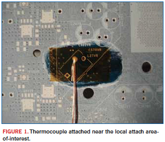
Attaching the thermocouples. The standard notes specific, preferred thermocouple attachment methods. A picture of the taping method, just off to the side of the painted land area-of-interest, is shown in Figure 1.

Best practice: Attach the driving thermocouple near, but outside, the package land area to be measured.
Fixturing the samples. The standard notes that there are various assembly fixturing techniques used in reflow assembly, including on-rails, simply supported (with at least one rail across middle), and different clamping methods.
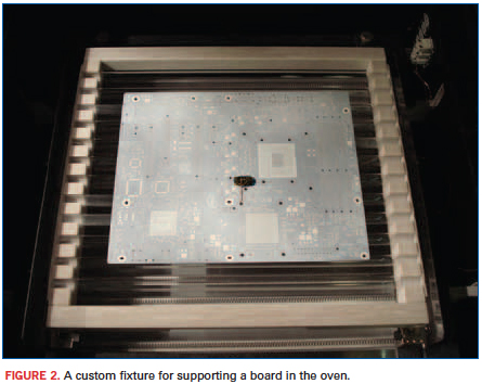
Not fully covered in the standard is what to do about measuring the boards if they are normally clamped during assembly. This is especially relevant, since clamping the boards does affect warpage, and putting a board that is in a clamping fixture into the oven of the measurement equipment will likely not work, if the fixture blocks heat transfer to the board. Many, but not all, measurement systems use IR heating, and if the clamping fixture blocks radiated energy, it will not be possible to measure the PCB in situ with the same mechanical constraints in place as when it goes through the reflow oven. Measuring with a simple support setup and using that data to correlate with what the area will actually do when clamped is one alternate approach. However, the sample is supported in the oven – with two or three rails, on a flat glass sample support, a specialized fixture (Figure 2), or in its own clamping fixture. This setup should be established and communicated with all the supply chain partners in your correlation group.

Best practice: Fixture boards consistently for all measurements.
Establishing the thermal profile and measurement temperatures. Another method you should share with all your supply chain partners interested in board warpage is the thermal profile and measurement acquisition points you will use for each board design. Comparing results both between and within board designs, for different regions of interest, is facilitated by establishing a common set of temperatures that are important for decision-making. Measuring at multiple points is prudent, but it can become impractical to attempt to measure at every single degree, for example, since temperatures are changing quickly and each measurement takes some non-zero amount of time to complete.
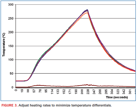
Ramp rate, or the rate of change of temperature of the sample, is mentioned in the standard. The standard recommends setting the ramp rate as high as possible, provided it does not induce more than a 10˚C difference between the top and bottom of the sample. In our experience, a 0.5˚ to 1.0˚/sec. heating rate is ideal; though, with thicker boards that tend to impede temperature equalization, the target rate will need to be established with actual test results per board design.
Best practice: A typical temperature profile with acquisition points is shown in Figure 3.

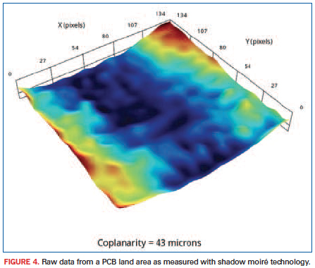
Taking measurements. After all this preparation, it’s finally time to take some measurements. The board is in the oven; the profile is set; the automated acquisition software is run, and the machine does the rest. An example of raw data from a PCB land area, measured with shadow moiré technology, is shown in Figure 4.

Best practice: Run the thermal profile, and obtain measurement data only at important temperature points.
Analyzing and reporting the data. Analyzing the raw data results by following a common method is required if data are to be correlated with other parties. The amount of data smoothing, data density and other variables need to be controlled as closely as possible to get the closest resultant correlation. Preparing results in a table or 3D visual reporting format are common ways that package suppliers communicate dynamic warpage. With enough samples measured throughout a temperature range, and associated analyses run, this complete process is sometimes called the warpage characterization of components such as packages and PCBs.
Best practice: Process data according to a common methodology shared among supply chain partners. Create template-based reports to share.
Number of samples. Establishing a statistically acceptable set of results will depend in part on how many samples are tested, of a given lot of a particular design. The standard recommends testing a minimum number of PCBs to establish the performance characteristics of the lot; although, testing more may give a higher confidence level that a representative range and standard deviation have been properly established. Generally, the warpage tendency of a particular PCB lot is usually clear once 10 samples have been measured.
Best practice: Test enough boards per lot to effectively “characterize” the lot’s expected warpage across temperatures.
In releasing IPC-9641, High Temperature Printed Board Flatness Guideline, IPC has indicated that making assumptions about the warpage of one side of that interface – the package land area on the PCB – is no longer sufficient for the design of reflowed assemblies. We are moving toward an era when the shapes of the components attaching during reflow will be compared and constrained at each temperature, and the compatibility of those shapes will tell us what needs to be done to get the best product yield, as well as what final quality level can be expected from their combination. Measuring the reflow-induced warpage of package land areas on PCBs is a big step in that direction.
Acknowledgments
Information about thermal warpage measurement best practices in this article was provided and reviewed by the subject matter experts at Akrometrix, Ryan Curry and Neil Hubble. John Davignon not only led the subcommittee that developed IPC-9641, but also reviewed and contributed the foreword to this article.
Ken Chiavone is vice president of engineering at Akrometrix, and is currently writing a book on warpage management; kchiavone@akrometrix.com.
John Davignon is founder, Davignon Consultancy, LLC, and Chair, Printed Board Coplanarity Subcommittee (IPC-9641).
Press Releases
- Horizon Sales Expands Consumables Portfolio with ROCKA Partnership, Bringing More Value to U.S. Manufacturers
- Libra Industries Appoints Gustavo Sariñana as General Manager of Guaymas Facility
- BTU International Appoints Performance Technologies Group as Exclusive Representative in Tri-State Region
- Kitron Inks 42M Euro Order From Defence/Aerospace Customer


