

Current Issue
A New SPI Tool for Defect Prevention
Component tolerances address paste imbalance on individual devices.
Solder paste deposit imbalance is a key factor in the formation of many reflow soldering defects, including tombstones, drawbridges, non-wet opens, head-in-pillow, and tilted QFNs. A new automated solder paste inspection (SPI) routine can check for paste volume imbalance to preempt the defects prior to component placement.
SPI machines measure solder paste deposit characteristics such as volume, height, area and position. Then they compare the values against programmed control limits. If all the values are within the control limits, then the print is considered a Pass; if one or more deposits are outside the control limits, the print is rejected as a Fail. The most commonly checked parameters are volume and position.
The control limits, or primary tolerances, are usually expressed as a percentage of the corresponding stencil apertures’ theoretical size and location, and can be programmed by a user or set automatically. Typically the default tolerances are +/-50% of their nominal, or CAD, values. They may be adjusted depending on specific devices. 0201 or 01005 components sensitive to tombstoning may run tighter limits. Large BGAs prone to warpage may use limits that are shifted higher to ensure a minimum amount of paste. Smaller BGAs more prone to bridging may use limits that are shifted lower to prevent excessive deposits or to compensate for partial paste release due to lower area ratios (low area ratio compensation can also be automatically included in the default tolerances when programming). These primary tolerances are referred to as “pad tolerances” because they consider each pad individually on a pass-fail basis.
The secondary tolerances – or component tolerances – consider all the pads in a component’s footprint in their pass-fail criteria. They examine the ranges of deposit characteristics on a per component basis and compare those ranges with programmed limits. The limits are defined as a percentage of the nominal value that the system expects. For example, a typical 0201 aperture is expected to deposit about 400 cu mils of solder paste on each of its two deposits. Under the traditional tolerance scenario of +/-50%, one pad could have 200 cu mils of solder paste, while the other pad has 600 cu mils, or three times as much. In this case of theoretical extremes, a tombstone is sure to occur. Even moving away from the extremes toward the center of the specification at 250 to 550 or 300 to 500 cu mils on the individual pads, the imbalance is still considerable enough to contribute to defect formation. FIGURE 1 shows the programming window for pad and component tolerances.
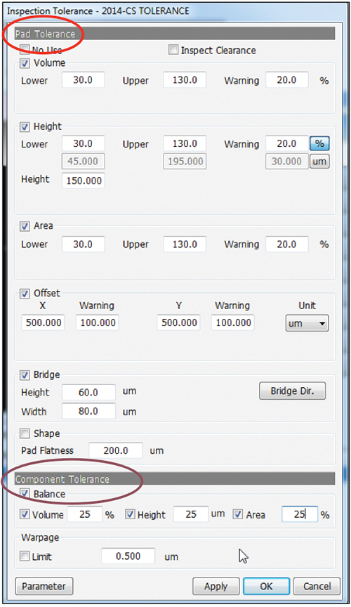
Figure 1. SPI tolerance programming window showing how pad and component tolerances are programmed together.
By adding a component tolerance, the programmer can ensure a good balance without over-constraining the primary control limits. Assume that a maximum 25% range in paste volume is desired on the 0201 – that’s 25% of the nominal 400 cu mils, or 100 cu mils. Both solder paste prints must be within 100 cu mils of each other, or the print gets rejected. They may be on the low end of the spec at 200 to 300, or pushing the high end at 500 to 600, but their range can be no more than 100 cu mils in order to pass at the component level.
Paste balance-related soldering defects. In addition to tombstones, drawbridges or non-wet opens on chip components, paste imbalance can also contribute to skewed components and mid-chip solder balls. On gullwing components, paste imbalance can contribute to opens, non-wet opens, solder bridges or solder balls. Solder defects on chip and gullwing devices are relatively easy to capture and repair because they are visible and accessible; however, BGA, LGA or QFN solder defects are more difficult and costly to identify and fix.
BGAs may have a few or a few thousand solder joints, and it only takes one bad one to force them all to be reworked. Deposits outside the range on the low end can cause non-wet opens, head-in-pillow, or thinner joints with questionable reliability. Conversely, deposits outside the range on the high end can cause solder bridges or excessive solder defects. Maintaining a steady range in deposit volumes will reduce rework and improve overall interconnect quality.
LGAs are very sensitive to paste volume imbalances. Unlike BGAs, where the bulk of the solder joint comes with the package, LGAs rely solely on the solder paste deposit to make reliable connections. If a BGA deposit contains 30% less solder paste than the neighboring deposits, the impact on solder joint volume is barely noticeable. If an LGA deposit has the same deficiency, the result is an open joint or a joint with a cross section at least 30% smaller than the neighboring interconnections. Keeping volumes consistent from pad to pad is critical to both the assembly process’ yield and the devices’ long-term reliability.
QFNs and other bottom-termination components (BTC) present numerous solder and inspection challenges, including tilting due to excess solder paste on the center pad or insufficient paste on the perimeter pads. Like LGAs, their interconnections depend wholly on the repeatability of solder paste deposits, and because of their varying pad sizes, calculating and maintaining a volume balance is absolutely necessary to achieve a consistent, reliable 2 to 3 mils standoff.
Component tolerances can also be set to monitor height measurements in order to identify peaks that may create slump-related problems like solder bridges or solder balls, or low spots that may exacerbate contact and wetting problems associated with non-coplanar component I/Os. Area ranges can be checked to ensure similar pad coverage and component contact to guard against wetting issues such as tombstones or skewed components, and component shifting issues from movement during conveyor transport or placement.
FIGURE 2 shows the SPI machine’s balance error warning message for a QFN that passes primary tolerance criteria, but fails component tolerance criteria. The height and volume ranges are both too high, and this print would likely cause reflow defects (tilting, insufficient or open) and reliability concerns.
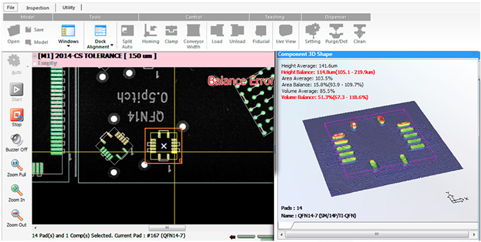
Figure 2. Solder paste balance defect on 0.5mm QFN.
Improved process control and troubleshooting. The component tolerance algorithm addresses the causes and effects of many SMT defects from an overall process perspective. Joe Perault, technical services manager of Parmi USA, explains: “As an industry, we have become very adept at eliminating gross print defects with SPI systems. This new level of control enables us to incorporate our broader process knowledge beyond the printer to prevent defects that occur downstream during placement or reflow.”
Component tolerances not only incorporate the ability to prevent downstream defects, they also enable engineers to better diagnose problems and achieve tighter levels of process control. Correlating end-of-line defects to solder paste print defects is not easy when all volumes fall within the overall primary tolerance. Correlating the paste balance-related defects with their associated value ranges focuses the data-mining effort and will reveal issues that can be easily rectified. Paste volume imbalance can have a number of root causes, including:
- Weak spot or uneven tooling support.
- Excessive PCB warp.
- Intermix of mask- and metal-defined pads.
- Gasketing issues.
- Stencil design.
- Errant paste drop-off from non-printing squeegee.
- Poor print parameters or finicky solder paste.
Solder paste balance is a very important contributing factor to SMT defects, and checking it does not add any cost to the process. The component tolerance algorithm utilizes data gathered in the regular inspection routine and therefore does not require additional cycle time, and the optional check is part of the standard software package.
Jeff Mogensen, general manager of Parmi USA, describes the impetus behind the paste balance feature: The component tolerance algorithm is a great example of how we incorporate intelligence into our systems.” Other intelligence-based features include diagnostic software that helps analyze root causes of print defects in real time, correlates them to screen printer activities and provides operators with corrective actions, and an on-board solder paste jet dispenser.
Summary
The component tolerance check adds a new level of sophistication to SPI without adding cost or cycle time. It provides the capability to compare characteristics of individual deposits with each other and enables tighter process control without the tighter pad tolerances that can cause “false” failures and slow the production line. This component-based comparison capability can prevent a myriad of defects in the PCB assembly process, for which paste imbalance is fully or partially responsible, and can quickly improve an SMT line’s productivity and profitability.
is founder of Shea Engineering Services (sheaengineering.com); chrys@sheaengineering.com. She wrote this on behalf of Parmi USA.
SIDEBAR
First Aid for Insufficients
Insufficient paste deposits are the leading defect detected by SPI. Some estimates hold that half the boards rejected are for insufficient defects that are repairable with solder paste jetting technology.
The jet dispenser is mounted on the SPI inspection head (FIGURE S1). Following the inspection routine, if the only defects found on the PCB are insufficient paste, the jet dispenses enough paste to reach the desired volumes. After dispensing the additional solder paste, the SPI system scans the deposits again to ensure the proper paste volume was achieved. If the print contains defects that cannot be repaired by the jet, such as excessive solder or bridges, the jet does not dispense and the board is rejected.
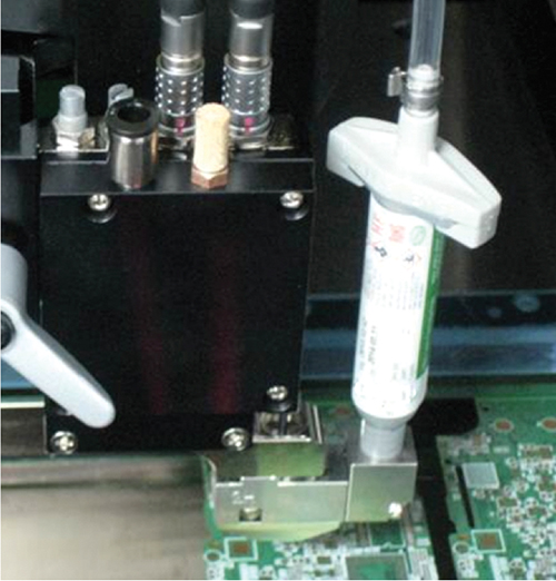
Figure S1. The SPI solder paste jet.
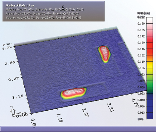
Figure S2. The SPI machine detects insufficient deposits…
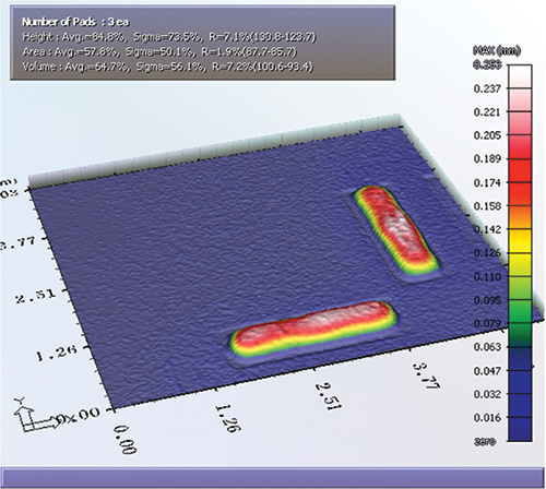
Figure S3. … And repairs the defective sites, then rechecks them.
Jetting “top off” solder paste to repair insufficient defects inside the SPI machine eliminates the need to clean and reprint the printed circuit boards. Doing so can reduce SPI reject, repair and scrap rates by as much as half.


Press Releases
- Seika Machinery’s SMI 2026 Webinar Series Continues with Focus on PCB Cleaning Before Solder Paste Printing
- Forwessun Expands Testing Capabilities through Strategic TRI Alliance
- Federal Electronics Expands Advanced Manufacturing Capabilities to Support Military and Aerospace Cable Assembly and Wire Harness Programs
- Altus Continues Irish Growth with Expansion of Engineering Team