

Current Issue
What You Cannot See Can Be Hand Soldered
Three techniques proved reworking the smallest parts is possible, given certain conditions.
With the advent of the ultra miniature 01005 body packages in a lead-free solder assembly environment, there is a need to develop an optimized process to rework these passives. Given their size – 10 x 5 mils or 0.25 x 0.125mm – it is no surprise that reworking 01005s with lead-free solder paste is a great challenge. In light of this need, a group of rework engineers put their collective thoughts together to review the most common possible solutions for reworking 01005s (FIGURE 1). In this experimentation, two applications labs with mostly different equipment sets evaluated a variety of different techniques for the rework of these 01005 components.
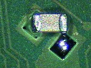
Figure 1. An 01005 component rotated off pad.
Numerous challenges are associated with the manual rework of 01005s. The greatest challenges include:
- Difficulty in seeing the component with sufficient magnification and optical resolution.
- Capability to allow in-situ process observation of the working area.
- Securing the component handling process from pickup from tape to placement.
- Controlling placement of fragile components with very low mass (0.04g/1000 pcs.) so as not to physically damage them.
- Force-controlled handling and placement throughout the entire rework process.
- Removing components to be reworked without disturbing neighboring devices.
- Hand-placing new components manually at at least 10µm accuracy.
- Dispensing solder paste or solder paste transfer with consistent solder volumes.
Some of the very specific challenges in manually reworking this package include:
- An extremely high level of dexterity required of the rework technicians due to the size of the components. As a point of reference, the pads are typically 3 to 7 mils (0.076 to 0.178mm) square with 2 to 4 mils (0.051 to 0.102mm) spacing to neighboring pads.
- The temperature ramp needs to be low, as the thermal mass of the components is small, and the heat-withstand properties are limited.
- Designs employing these devices have tight spacings to control with even the most dexterous person; some parts are spaced 0.2mm or less.
- Control of the solder volume needs to be such that a very small volume of solder paste needs to be placed consistently and controllably on very small pads.
- Site cleaning is treacherous, as even the smallest of forces can lift the pad.
Experimental Procedure
The following three processes were investigated as potential manual 01005 package rework methods. Each method was investigated, documented via photos and video (see the “Solderinggeek” channel on YouTube for the methods) and the results inspected per IPC-A-610E. Finally, the methods were rated on a variety of attributes. Semi-automated machine approaches were not considered as part of the scope of this work.
Solder ball and fixture technique. In this method, the challenge of maintaining a correct and consistent solder volume for these component body styles is overcome with the consistent solder volume found in a solder ball. After gel-fluxing the pads, the component is placed on the pads. The smallest of the special tools is selected for use. A Kapton flux dip tray is used, which controls the amount of gel flux deposited to the watch oilers. They are dipped vertically in either a 0.1 or 0.15mm flux dip tray.
After the part has been picked up and placed under a microscope with the watch oiler tool, the solder balls are placed. Again, the tool of correct size is dipped vertically into the flux and then positioned above the solder ball matrix, where the solder balls have been separated by a Kapton matrix (FIGURE 2). By simply touching the ball, it can be individually picked from a matrix and presented to the component, where the ball will stick to the pad (FIGURE 3) and the component using the surface tension of the flux on the PCB. The balls are placed on the end of the pad (FIGURE 4) and reflowed using a low airflow velocity hot air (FIGURE 5) or IR source so as not to disturb the solder joint during reflow.
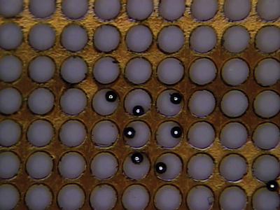
Figure 2. Balls are loaded into apertures.
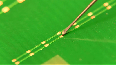
Figure 3. Flux dispense rotate oiler to pads.
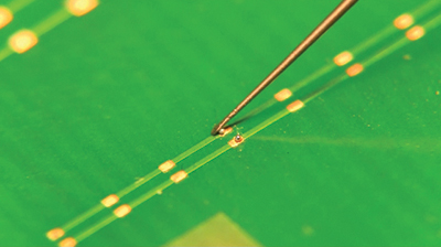
Figure 4. Place solder balls after dipping in flux tray.
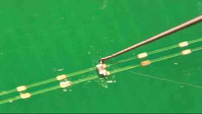
Figure 5. Place part, then reflow with low air velocity reflow source.
Hand soldering. The second method investigated for the placement and reflow of the 01005s was completed by a highly skilled soldering technician using traditional conductive hand soldering tools (FIGURE 6).
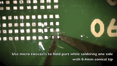
Figure 6. Hand soldering an 01005 using a steady hand.
Plastic fixturing and stencil printing technique. The final technique investigated the plastic stencil and part holding technique, using a modified version of the stencil printing rework method for placement and reattachment of the 01005. After site prep, pads were printed with Type 4 solder paste using a special adhesive-backed stencil. This is followed by component placement using a part placement stencil to align the miniature device package on the pads. Finally, the device is reflowed and inspected (FIGURE 7).
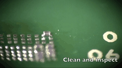
Figure 7. Clean and inspect.
Each rework process step for these ultra-miniature packages requires a high degree of care.
In the desoldering process, the degree of precision with respect to the heat applied does not have to be as exacting, as the removed parts are of very little economic value and in nearly every case scrapped. If a hot air source is used, then it is imperative neighboring ultra-low-mass and footprint parts are not disturbed.
Care must be taken in the removal of residual solder during the site preparation step of the rework process. Improper solder wick techniques can scratch the mask or lift the pads. A noncontact desoldering approach can avoid these potential pitfalls. In addition, the operator, independent of the process used, needs to have a steady hand and not disturb nearby components during site preparation.
A repeatable, flexible method is required for solder paste deposition. Due to the component size, the typical hand soldering process using wire cored solder is not very controllable.
Component placement requires a steady hand so as not to disturb nearby components or smear solder paste all over the board.
For the reflow process, controlled heat with minimal airflow is required so as not to disturb nearby components. These ultra-miniature heat-sensitive components, like capacitors and LEDs, can be easily damaged. In addition, the heating ramp rate needs to be limited or components can crack or incur thermal damage. This can be limited by a combination of controlled heat sources and by preheating the PCB.
Results and Analysis
For each method a variety of advanced soldering technicians used a variety of hand tools and fixtures, as well as components and boards to rework the 01005s. Each of these efforts was documented using process photographs, and a combined “usability” score for each method was developed (TABLE 1).
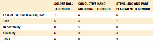
Table 1. Comparison of Usability Scores for Hand Soldering 01005s
The usability scale used the following ratings:
- Ease of use, skill level required. 1 (most experienced, only the most advanced soldering techs could perform) to 10 (least experienced, beginner skill level could perform).
- Time. 1 (quick process) to 10 (lengthy, drawn-out process).
- Repeatability. 1 (highly dependent on skill level of operator) to 10 (highly repeatable process).
- Flexibility. 1 (dedicated tooling; need new tooling every time attributes change) to 10 (can be used independent of location on board).
- Tools. 1 (uses completely new tool set) to 10 (uses essentially the same tools).
A Practical Components immersion silver finish 01005/0201 development board using a SAC 305 solder with a no-clean flux chemistry was used for the trials, unless otherwise noted.
The solder ball and fixture technique was performed on several site locations. An Alpha 033 no-clean gel flux was squeegeed into a dip tray. The 4 mil depth section was used for the 8 mil solder spheres, and the 6 mil dip tray was used for the 12 mil solder spheres. The hand tool was dipped into the flux, with flux transferred to the pads of the component. The component was dipped into the flux and placed on the fluxed pads, centering them to the pads. The solder balls were dipped until they bottomed out at the bottom of the dip plate, and placed with the oilers dipped into flux dip tray. The balls were picked up using the surface tension of the flux from the Kapton matrix ball holder. Finally, one solder ball was placed on each end face of the component on the pad.
When the component or solder ball is touched to the PCB, it will not move due to surface tension differences. Make sure to select the oiler size best-suited for the job.
Ensuring use of the correct solder ball sizes/volume of solder is critical to ensuring all solder joint criteria for this device body style can be met. Like all these manual methods, the inherent downside is its dependence on the skill level and dexterity of the rework technician. In addition, this method requires the use of several new specialty hand tools that allow pickup of the components, solder balls and the application of the flux.
There were several advantages to this particular rework approach. The use of solder balls ensures consistent solder volume. The gel flux used is very advantageous when it comes to holding the device and solder balls in place. In terms of first-pass yields, there were few yield detractors outside of the skill level and (calm) touch of the rework operator.
Hand soldering of the 01005 package was performed using a power supply and a 0.4mm bent conical conductive tip. In addition, specialty hand tools such as an Exacto knife, an ESD-safe pair of tweezers and a dental pick were employed. The technique focused on the “topside” removal process, where the tip touches only the top of the component, thereby allowing solder surface tension to lift the component out of the way. After turning on the soldering station power supply and making sure the tip was tinned and at temperature, a small amount of solder was cut from a 0.5mm diameter cored wire Alpha SAC 305 solder using an Exacto knife the approximate size of the pads. These small pieces of solder were then placed on the pad and a small amount of Alpha 0M-338 gel flux was then added. Using a pair of tweezers, the 01005 package was placed and aligned. Next, the component was aligned to the pads.
While holding the component with a static safe pair of tweezers, the 0.4mm diameter beveled soldering tip was contacted to one side of the pad to permit the component to reflow. The other side of the device/pad was then contacted with the tip. Finally, the reworked location was cleaned and inspected per the proper inspection criteria.
One challenge in this technique is the control of the placement force (like the other manual techniques described herein), as a force in excess of approximately 200g can cause component cracking. It also requires very advanced soldering skills. Because components such as ceramic capacitors and LEDs cannot be subjected to the temperature gradients with the direct conduction heating method, its applicability is limited. Last, since the amount of solder applied to the part is very small, it is very difficult to control solder volume consistency, and hence, solder fillet quality.
This technique has several advantages. First, it is very similar, albeit for a few newer tools, to other micro-component soldering. Second, no solder paste is applied on an assembled board that could potentially cause shorts.
The final technique investigated was stenciling and part alignment stencil. First, the backing of the transparent printing stencil was removed. The stencil was then placed onto the board, aligning apertures over pads to be soldered. Using a micro squeegee tool, Alpha OM-338 Type 4 solder paste was rolled into the apertures, making sure they were filled. The printing stencil was then removed. At this point the print was inspected to ensure the apertures had consistent solder paste volumes. Next, the amber-colored alignment stencil was placed over the just-squeegeed pads, with care taken not to smear the solder paste. Using a pair of micro tweezers, the part was then placed into the alignment aperture of the alignment stencil. With the proper reflow source, the solder was then reflowed. Finally, the site was cleaned and inspected per the appropriate criteria.
Challenges using this technique included proper placement of stencils and smearing of solder paste. Due to the size of the stencil and the proximity of the to-be-reworked location relative to other components, proper placement of the flex printing stencil is difficult. In addition, any time a PCB repair technician is working with solder paste on an already-built board, there is the possibility of smearing the paste and causing shorts.
There are several advantages of this particular rework approach. One of its benefits is the consistency in solder paste volume deposition. This helps create a consistent fillet, which is key in soldering these ultra-miniature devices. The part placement stencil helps reduce the dexterity required for device placement, thereby making this technique more feasible for those with lesser hand-soldering skills.
Conclusions and Future Work
While there are numerous rework techniques for a variety of package sizes, the 01005 represents many new challenges for rework technicians, including but not limited to being able to control solder volume, the small part mass that makes most convective tools “blow away” components, and the existing tools, which are not suitable for part and material handling. Each of the methods investigated proved a viable option for reworking 01005. Each rework method resulted in the proper solder fillets, given the inspection criteria, and each required different operator skill levels and new fixturing or tooling to make them work.
Conductive hand soldering was the least desirable method, as it has limited use, given that several components cannot withstand the temperature ramp rates. The stenciling approach is cumbersome, as different stencils need to be custom-fabricated and placed onto the board. Also, the use of solder paste in a rework operation may not be allowed by some EMS companies, as its poor control can lead to errant shorts on the boards after rework. This leaves the solder ball method as the most consistent, most flexible method of those investigated for the manual replacement of 01005 package sizes.
While a pin transfer technique (FIGURE 8) was initially considered as part of this work, time constraints and a lack of proper tooling prevented this method from being investigated. Proper investigation of this method will need to include a variety of different solder pastes in order to optimize the process. In addition, a variety of pin and pad geometries need to be investigated, along with the development of a means to align and deposit the paste onto the center of the pad.
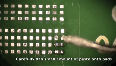
Figure 8. Attempt at pin transfer technique using small tool. (Photo courtesy Nordson YesTech)
Bibliography
1. Ronald Wachter, “01005 Passive Component Rework,” SMTA International, October 2013.
2. Norbert Heilmann, “01005 Assembly Process – From the Board Design to the Reflow Process,” IPC Apex, April 2008.
3. Chrys Shea, Leszek Hozer, Ph.D., and Hitoshi Kida, “A Feasibility Study of 01005 Chip Components in a Lead-Free System,” SMTA International, October 2005.
4. Rita Mohanty and Vatsal Shah, “Assembly Process Challenges for 01005 Components,” SMTA International, August 2008.
5. Mike Berry, “Optimization of the 01005 Discrete Assembly Process,” International Conference on Soldering & Reliability, May 2011.
6. Galen Alexander, “AOI in an 01005 World,” International Conference on Soldering & Reliability, May 2011.
7. M. Berry, ibid.
8. Paul Houston, Gary Turpin and Daniel Balwin, Ph.D., “Implementation of 01005s: A Case Study,” SMTA International, August 2008.
9. Joe Belmonte, Vatsal Shah and Rita Mohanty, “Process Development for 01005 Lead-Free Passive Assembly,” SMTA International, September 2006.
Acknowledgments
We would like to thank James Barnhart and Hung Hoang of BEST Inc. for their work on developing several of the photographs and processes.
is Advanced Product Applications Manager at OK International (okinternational.com); pwood@metcal.com. is president of BEST Inc. (solder.net); bwet@solder.net.


Press Releases
- Niche Electronics Celebrates Completion of Florida Expansion
- Microscreen Names Nik Thomas Director, Expands Leadership Role Amid Continued Organizational Growth
- W&S Enters New Growth Phase Through Strategic Partnership and New Leadership
- Federal Electronics Expands Environmental Testing Capabilities with New Extended-Range Thermal Test Chamber