Current Issue
Refining Lean NPI at Optimum Design Associates
After two years of implementation, an EMS has virtually eliminated project “callbacks.”
This paper is the third in a series that describes the ongoing journey of Optimum Design Associates from initial concept and planning through our implementation of Lean NPI. This third paper examines data from before implementation and compares them to the data that have been compiled over more than a year of using Lean NPI as a best practice.
Optimum is an EMS company that provides design and layout services along with full turnkey PCBA manufacturing. Having all of this in-house gives our design team the perspective and understanding of both the electronic and manufacturing requirements to implement a successful design.
As background, we have discussed in two previous papers the then-current business practices at Optimum, including the design flow and integration of layout and DfM tools, and the process of setting up and launching our Lean NPI program1, and described why and where processes can be implemented to align Optimum with the best practice Lean NPI model, along with metrics for tracking and measuring progress.2
First, a quick refresh on the best practices Lean NPI model as defined by Optimum. In the model, there are three critical elements to the Lean NPI model.
The first integral part of the model is using an intelligent manufacturing data transfer method. Our preferred method is to use ODB++ for every customer we can. The format permits quick importing of all necessary manufacturing data from the PCB CAD software to the CAM tools.
The next important element is concurrent DfM during PCB design. This means incremental DfM checks can be run at various layout milestones, such as placement approval, critical routing, full copper connectivity and final approval.
Third, perform Level 2 DfM as defined in the previous papers. This means adding specific vendor rules into the DfM rule set. This ensures the board fabricator’s rules
are followed.
Program Goals
As an ISO certified supplier, we made Lean NPI a continuous process improvement (CPI) initiative. Representatives from manufacturing, layout and the quality team set the goals we wanted to achieve. As with any CPI, the overall goal is to improve yield and reliability in the most efficient manner possible. Our Lean NPI program goals are:
- Streamline the process of preparing and delivering intelligent manufacturing data files.
- Find DfM issues in layout as close to real time as possible.
- Fine-tune the DfM rules (ERF files) to match Optimum’s and our vendors’ capabilities.
- Define a set of metrics to track and measure continuous quality improvement. The goal is not necessarily to see numbers trending down, but to call the designer’s and customer’s attention to potential issues that can affect PCB yield and reliability.
In Optimum’s Lean NPI process, the first step is to validate the bill of materials (BoM). We use Mentor Graphics Valor NPI and Valor Parts Library (VPL). This ensures that all the part numbers, reference designators and quantities are correct, and VPL package models are available for later use in the design flow. Next, components are placed and a DfA is run. Results from the DfA are incorporated into the design, and the rest of the design is then completed.
After the customer has reviewed and approved the design, a full DfM analysis is run and results reported to our designer. Any issues are fixed in the design, and DfM checks are run again until clean. A final package is then released to be manufactured.
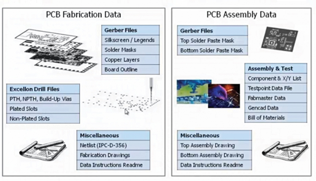
Data transfer. The ODB++ manufacturing data transfer method is important to the implementation of Lean NPI at Optimum. Since concurrent DfM involves moving DfM to as early in the project as possible, it is essential to perform the DfM checks as quickly as possible to maintain very tight schedules. Using ODB++ frees time previously used to set up the myriad files for these DfM steps too. FIGURE 1 illustrates all the files required using Gerber and the adjunct files also required, as compared to a single ODB++ file.

Figure 1. Using the Gerber format required more than 30 files to contain all manufacturing data.
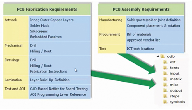
The ODB++ file itself is really another CAD database that is made up of all the necessary files, organized into folders and compressed into a single .tgz file, so everything the manufacturer needs is contained in a single file. FIGURE 2 shows the structure.

Figure 2. A single ODB++ file is a CAD database that comprises a compressed set of the entire manufacturing data set.
To ensure all the data were accurately embedded into the one file to manufacture a PCB, we embarked on an evaluation where we added a step into our standard process to check the ODB++ file against Gerber data. This was performed using the Gerber Compare feature in Valor NPI. Over the course of about six months and a little over 100 design deliverables, we found confidence to move completely over to ODB++ for all future designs.
The second goal was to move DfM earlier in the process. In doing so, we were able to add two new fabrication analysis steps. The first is after critical nets have been routed. This finds any problems with those important nets as early as possible, providing the opportunity to rectify them quickly and inexpensively. The second added check is when we have full copper connectivity. Now, knowing that the critical nets are manufacturable, the DfM step checks for errors in the balance of the design, and of course checks to see that nothing has been “broken” with the rest of the layout. Speed is the key to be able to do this (both speed of setting up ODB++ and also running the checks).
This brings up the third goal: fine-tuning the rules. The Valor tool comes with almost 900 rules (ERFs) out-of-the-box, and for the most part they are pretty good; however, as a contract manufacturer we felt the need to fine-tune these rules to better match our internal processes. In the case of fabrication checks (DfF), our approved suppliers provide and allow us to use the same ERFs that they use internally.
On occasions where we design a PCB but don’t necessarily know which vendor will be fabricating it, we have a set of rules that best match all vendors’ requirements. Our rule files are then reviewed quarterly by our team representing layout, manufacturing and quality based on Valor NPI and assembly post-mortem reports. This allows the team to continually update our rules to eliminate any errors found, in order to improve yield and reliability, and reduce the number of flagged checks during DfM.
Measure and Compare
Data have been collected throughout the implementation of the Lean NPI process. These data are used to improve quality, reduce errors and identify areas for improvement. By observing violations found during DfM checks performed at Optimum, we can identify common issue trends. We can then educate our designers and find ways to mitigate the problems in our designs before manufacturing begins. For example, use of solder mask-defined pads has become more popular and important to design success as features shrink. Our layout designers are continually improving their skills as we receive a steady stream of DfM feedback with each new design we complete.
The goal with Lean NPI is to eliminate projects from going on hold and to improve the yield of each board released to manufacturing. Optimum has compiled statistics since implementing Lean NPI in the fourth quarter of 2012. Those statistics tabulate the design errors by type and severity. The most severe in Optimum’s judgment are callbacks, that is, when the supplier stops a project because of an error that would compromise yield or quality.
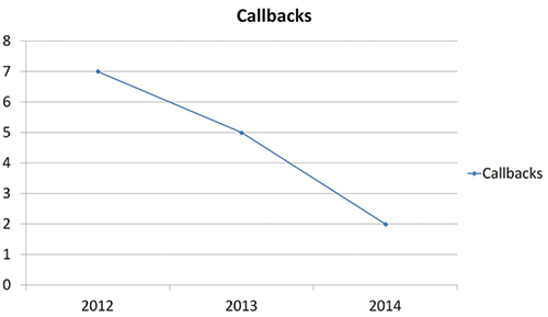
Looking at the history, we can see a downward trend of vendor callbacks that would inhibit the progress of the project. Virtually all show-stopper issues have been eliminated, and we have only the occasional review of less-critical items, such as suggested stackup modifications, fab note conflicts, or other minor topics that we are asked to review. As Optimum has gained experience with DfM, the number of all callbacks has been reduced to fewer than one per quarter, and those were “suggestive” issues: items that did not require artwork change. And while callbacks have been reduced, the number of designs has been gradually increasing.
In 2014 Optimum Design started offering Valor DfM checks as a service to our customers and also began a very proactive role in running DfM checks on all new, incoming assembly projects (not just PCB layout). These designs undergoing DfM checks have been created by outside companies and may not have followed Optimum’s preferred layout practices. These additional designs have greatly increased the number of DfM checks performed quarterly and the number of violations found. As seen in previous years, Optimum’s mature layout process and experience gained from DfM feedback has resulted in fewer violations found (FIGURE 3).

Figure 3. Since introducing Lean NPI in the fourth quarter 2012, the number of callbacks has steadily decreased, and no “show stoppers” were been logged in 2013 or 2014.
The most revealing statistic in the data compiled is the number of defects discovered per report. This number normalizes the data to eliminate skews due to the increased number of projects checked. Again, the most important errors are the ones that cause the project to halt – the “show stoppers.” TABLE 1 shows the number of design reports per year, the number of defects, plus the ratio of defects per report.
Table 1. Defects Per Design Report, 2012-14
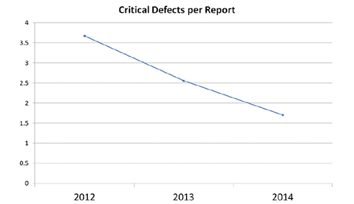
The graph in FIGURE 4 clearly shows the expertise that Optimum has acquired is paying off. The number of “critical” class errors decreased from 3.67 per report in the fourth quarter of 2012 to just 1.70 per report in 2014. This indicates that as Optimum’s experience with Lean NPI grows, the designers ensure major problems are avoided during the design itself.

Figure 4. The number of critical defects (show stoppers) per report shows a reduction of more than 50% in just over two years.
Another indicator that validates the ongoing Lean NPI investment is the amount of time spent on each project readying it for production. Before Lean NPI, most data files submitted to Optimum used Gerber PCB data and supplementary files with manufacturing data. One part of the implementation process was to move as many designs as possible to ODB++, which packages the complete set of manufacturing data, as well as the PCB design data. TABLE 2 summarizes the significant improvements recorded during the past two-plus years.
Table 2. Time Allocations Based on Data Transfer Format
Ongoing Plans
Optimum has implemented Lean NPI and has now been using the model for more than two years. At this point, we have great confidence in ODB++, but we still have to offer Gerber to a few customers that have not changed over. The supporting data indicate, despite undertaking more DfF checks for customers, we have been able to continue decreasing the number of critical defects. And, it is taking much less time to deliver higher quality designs.
Since moving DfM earlier in the process, we are catching errors much sooner than ever before, allowing them to be quickly and inexpensively rectified. Additionally, the review and updating of rule files have also shown positive benefits. Implementing Lean NPI is helping ODA achieve our quality and reliability goals at the lowest cost possible.
References
1. “Lean NPI at Optimum Design Associates: Where Are We Now?” company white paper.
2. Randy Holt, “A Lean NPI Journey,” PCD&F, July 2013.
is a senior PCB designer at Optimum Design Associates (optimumdesign.com) and a former “Top Gun” winner at PCB West; rholt@optimumdesign.com.
Press Releases
- Eastek International Corporation Appoints David Strabel as Vice President of Manufacturing
- SEMI Projects Double-Digit Growth in Global 300mm Fab Equipment Spending for 2026 and 2027
- Koh Young Announces Two Sales and Service Changes to Strengthen its Customers in the US and Canada
- Express Manufacturing, Inc. (EMI) Promotes David Vue to Lead Military and Aerospace Division


