Current Issue
ESD Concerns with PCB Assembly: Barcode Labeling and Masking
Overcoming charges and decreasing risks introduced by humans or machines.
An electrostatic discharge event can cause physical damage (e.g., surface oxidation, material loss) to circuits, either printed on the PCB or embedded in a component. ESD can also result in latent defects, resulting in reliability concerns. Many components are vulnerable to ESD; they include microcircuits, discrete semiconductors, thick- and thin-film resistors and piezoelectric crystals. All need precautions to prevent damage from an ESD event.1,11
The ESD problem in electronics production, especially PCB assembly, is significant. ESD damage can be seen immediately during assembly when a circuit stops functioning, or later in the life of the device. This latent ESD failure adds to the “cost of ESD” with repair costs, return costs, and end-user disappointment. Estimated product losses due to ESD are up to 7%.3
To understand the static problem, it is important to understand where static comes from. The main source of static comes when two dissimilar surfaces are brought into contact and then separated. The charge imbalance on each of the separated surfaces creates an electrical potential that may enable that charge to subsequently move. In PCB assembly, several key processes create triboelectric charge; they include human contact, machine contact (conveyors, robotics, etc.), applying solder paste, component mounting, tape masking and barcode labeling. All sources require consideration when developing an ESD control program.2,6,7
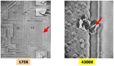
Figure 1. ESD damage (left); C2 MOS microcircuit damage.14
The first step taken by a PCB designer is to determine the sensitivity of the PCB and components to electrostatic discharge. Often the designer will rely on data supplied by suppliers (i.e., component manufacturers) for ESD sensitivity levels. These manufacturers will characterize sensitivity based on exposure to humans and machines. They will use models such as the human body model (HBM) and charged device model (CDM) to classify ESD sensitivity. In simple terms, the main difference between the two models is the rate of discharge with the human body releasing charges slower than when metal-to-metal contact occurs in the CDM events. However, even if humans and machines have the same 5kV potentials, the rate of discharge is slower for the human, and components may react differently to the different discharge rates.1,8,11
For example, a CMOS component may have a sensitivity of 1000V for the HBM, but only a 500v CDM. PCB and component manufacturers may use the ESD threshold classification to characterize their parts. Appendix 1 shows ESD sensitivity for a Texas Instruments Load Switch that has ESD sensitivity levels of 2kV and 1kV for HBM and CDM, respectively. TABLES 1 and 2 used in the ANSI/ESD/JEDEC JS-002-2014 standard contain the HBM and CDM threshold classifications.17, 22
If a PCB designer is using electronic components that are deemed HBM class 0B or CDM class C0b sensitive, a robust ESD control plan is needed. That plan would need to consider all aspects of PCB assembly and make sure three key elements are defined and resolved.9 They include:
a. All conductors need to be grounded. A charged, isolated conductor can be a dangerous risk.
b. Nonconductors (insulators) need to be replaced with static dissipative/low-charging materials whenever possible.
c. Transportation of the device outside of ESD protected areas (EPA) requires static protective materials (static safe packaging).
TABLE 1. CDM ESDS Device Classification Levels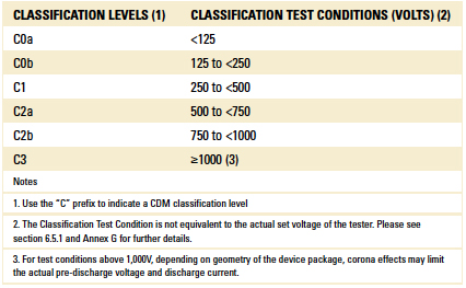
Table 2. Peel Voltages for Adhesive on a Tape and Label with and without Low-Charging Features15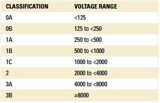
ESD Source: Masking Tape and Barcode Labels
For this article, we will consider in depth the role masking tape and barcode labels have in creating risk of an ESD event and steps that can be taken to reduce this risk. Both materials play an important role in electronics assembly.2,3,4,5,11 The masking tape provides protection to components during the assembly process by covering or masking sensitive components from flux, solder, and cleaning agents. The barcode label is important for providing a tracking method for PCBs during assembly. Most robust manufacturing processes collect data on the PCB during each assembly step and allow lot tracking via the barcode. Using a label printed on-demand at the site of manufacture offers a cost-effective and flexible way to barcode the PCB.
For assembly, the label and tape are typically cut into small shapes and are constructed of a film and adhesive that is supported on a release liner. Since the PCB goes through a harsh set of conditions, including high temperatures and harsh chemical exposure, the tapes and labels use a high-temperature film such as polyimide or polyester. Typically, the label will have a white coating to which ink adheres and provides contrast for scanning the barcode. Similarly, the tape may have a functional coating on the surface of the polyimide film. FIGURE 2 is a typical cross-section of a PCB masking tape and barcode label.
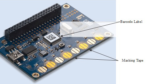
Figure 2. PCB with label and masking tape.
Both the label and tape produce similar static discharge concern(s). Before being applied to the PCB, both the tape and label are removed from the release liner. This can be done manually or automatically with a machine. By its nature, the adhesive and liner are poorly bonded, which permits easy release when separating. This poor bond is achieved by using a coating on the liner that is chemically dissimilar to the adhesive. The dissimilar chemistry causes a poor “wetting” of the adhesive that yields the poor bond. However, the dissimilar nature of the adhesive and liner has a negative effect in that they may produce a significant triboelectric charge when separated (or pulled apart). So, during the application process, the charged adhesive will induce a charge in conductive items (including circuitry). Measurements of charge potential of label and tapes removed from the liner can be greater than 5kV, depending on size.
A complicating factor to this triboelectric charge on the adhesive during the application process is whether the label is applied by hand or by machine. Any charge introduced by the human or the applicator machine can add to the charge potential of the label or tape and increase the discharge risk. In addition to this apparent risk, because the label/tape is a charged insulator, it can create a secondary problem. The charge has the ability to polarize the charge on the PCB or device. In other words, the PCB or device could have a neutral charge, but when the charged label/tape is brought into proximity, it will cause the opposite charge to move to the charged label or tape. This “field-induced” charge imbalance on the PCB or device creates a risk of discharge if the PCB is subsequently grounded at the inopportune time.
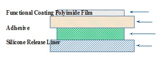
Figure 3. Barcode label and masking tape cross section.
Another concern with tapes and labels applied to a PCB occurs after application and during the life of the board. When the tape or label is applied to the PCB, it can be a source for charge accumulation. As mentioned, both the tape and label surfaces are either polyimide or have organic coatings that are inherently insulative (i.e., nonconductive). As a result, when the PCB is handled or moved – and the tape or label surface is contacted by conveyor, human, or robot – there is risk of charge building up on the surface that has the potential for enabling the polarization process described above, which in turn may lead to induction charging and discharging.
Typically, the barcode label is applied for the life of the PCB. However, in some cases, the label is removed. For example, when a PCB is made by a contract manufacturer, and the PCB is shipped to another company for final assembly in a device, the label may be removed. In the case of a masking tape, its function is to cover and protect an area on the PCB during assembly. At the end of the process, the tape is removed. The removal of the tape and label provides an ESD concern as charge is created during its removal. The PCB has dissimilar triboelectric charge potentials than the adhesive, and thus a charge can be created on the PCB and the adhesive during removal that needs to be considered in the ESD control plan.
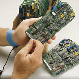
Figure 4. Application of PCB label by hand.
Countermeasures: Antistatic (Low Charging) Tapes and Labels
To address these static issues with masking tapes and/or barcode labels, an ESD control plan should consider “specialized” tapes and labels that have low-charging and static dissipative properties. Both properties will reduce the ESD risk. The following is a description of key tape and label properties and measurements:
Low-charging adhesive systems. As mentioned, a key ESD concern is the static charge that is created on the adhesive when it is removed from the liner. The dissimilar nature of the adhesive and liner allows for the adhesive to easily release, but also generates a significant triboelectric charge. To eliminate this charge buildup, several techniques can be employed independently or together:
Matching chemistries. By using an adhesive and liner release that are chemically similar and also closer on the triboelectric series of materials, you can decrease the charge buildup. While this is theoretically possible, it is difficult to find a system that is chemically similar and will function effectively in the application.
Conductive fillers. By adding conductive fillers to an adhesive, charge will move through a conductive path in the adhesive to a ground, so as charges develop, when the liner is removed, the charge is removed from the surface of the adhesive. The concern with this technology is that applying a conductive adhesive to the PCB may introduce a short or current leakage to any exposed circuits on the PCB or component.
Electric field shielding. When the liner is removed from the adhesive, the resulting charge buildup on the adhesive and liner produces an electric field that surrounds the charge. If shielding is applied in the proximity of that separation process, the charge will be reduced. The challenge with this technology is adding shielding may not be physically possible.
When these types of features are employed in a label or tape, the resulting reduction in charge buildup on the adhesive can be significant. A common measurement method of this charge buildup is to use a static field meter to measure the electrostatic field potential at a fixed distance from the charged surface.13 This electric field is measured in volts. TABLE 3 shows a comparison of charge buildup in volts for a tape adhesive with and without antistatic design features. As you can see, the measured voltage of labels and tapes with antistatic features in the adhesive is significantly lower than without the features.
Table 3. Peel Voltages for Adhesive on a Tape and Label with and without Low-Charging Features15
Static dissipative label face.4,6,7,12 After the label or tape is applied to the surface of a PCB, the insulative face can become a location for charge buildup, especially when handled and/or contacted by conveyors, etc. A key way to prevent this charge buildup is to make sure the face will allow charge movement over the surface of the tape or label and/or to a ground point. The charge movement should not be fast, but rather gradual so a large electric current is not introduced into the PCB.
The key measurement for charge movement or dissipation is the ANSI ESD STM11.11 standard test method, which details the measure of surface resistance. In the standard test method, surfaces are characterized by the speed at which charges move across them as follows: conductive (rapid), dissipative (slow), or insulative (minimal/none).
TABLE 4 shows surface resistances that relate to the surfaces.
Table 4. Surface Resistances for Material Types
The behavior of a charge placed on these surfaces is depicted in FIGURE 5. If a charge is introduced to a surface by triboelectric charging, it will produce a different level of charge density that will behave differently depending on the surface type.
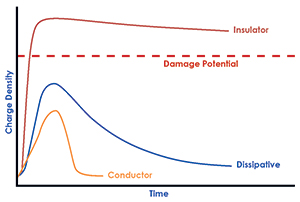
Figure 5. Static charge density and decay versus surface type.
As noted in Figure 5, if a charge is placed on an insulative surface, it will create an immediate high charge density at the point of contact, and that charge will have minimal decay over time. If an equal charge is placed on a conductive surface, it will not produce a high charge density because of its rapid dissipation across the surface through electrical conduction. This rapid movement of charge can also cause damage to static-sensitive devices if the current exceeds design limits. On a dissipative surface, the charge density will be initially lower than on the insulative surface and immediately begin to dissipate slowly across the surface.
The dissipation speed helps prevent both high charge densities and rapid discharges and safely neutralizes the charge.
The rate of charge movement is important. As stated, a rapid static discharge can be extremely destructive, causing a loss of material or chemical degradation at the point of charge impact as seen in Figure 1. Secondarily, a rapid charge movement can cause degradation of a circuit. Examples include gates (switches) used in diodes and transistors that can be damaged by exposure to high voltages, reverse voltages, high current or reverse current.16 This is often called electrical overstress (EOS). Thus, a rapid charge movement (i.e., high current) is to be avoided. FIGURE 6 depicts the rate of charge movement (decay) for each surface type.
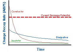
Figure 6. Charge decay rate versus material type.
Low-charging release liner. A third and equally important aspect of tape and label constructions that needs to be considered in an overall ESD control plan is the release liner. While the tape and label is removed and applied to the PCB, the liner also has a static charge from both the separation process of the adhesive and during handling. With respect to handling, this is often an under-considered factor in a static control plan. With either human, or machine (auto) application of the tape or label, a significant charge can be created on the liner. If not managed, the charge could be introduced into the environment and become a source of induction charging.
For the auto application of PCB labels, it is common to use a thin polyester liner to help with the fast application process. However, the polyester liner can generate significant charge. Using a liner that has a low tribocharging release coating (won’t develop a charge) and is static dissipative on the back side is key to managing ESD concerns with the liner.
TABLE 5 shows the benefits of using a low-charging liner for label and tape applications by indicating the electric field potential measured on the liner and tape/labels with a static field meter.
Table 5. Static Measurement for Label Face and Liners
Conclusions
ESD is a major threat to meeting the short- and long-term performance and reliability requirements of an electronic device. During the manufacture of the device, and especially during PCB assembly, a robust ESD control plan is an absolute requirement in order to mitigate the risk of ESD failures.
A key element of the successful ESD control plan is managing use of charged insulators (e.g., plastics) inside the production environment. Two common, charged insulators are barcode labels and masking tapes that are widely used for tracking and protection of electronic devices, respectively. Through use of low-charging and static-dissipative features on tapes and labels, the risk of ESD can be reduced.
References
1. EOS/ESD Association, “Fundamentals of Electrostatic Discharge; Part 3 – Basic ESD Control Procedures and Materials,” In Compliance, October 2010.
2. How Does Electrostatic Discharge (ESD) Relate to Labels? Polyonics white paper, 2003.
3. Justin Bergholtz and Vicki Heideman, “Understanding and Avoiding the Costly Effects of ESD,” Rockwell Automation Journal, June 2014.
4. Jim Williams, Thoughts on Surface Resistivity Issues in ESD Label Materials, internal Polyonics memorandum, December 2009.
5. Jim Williams, Thoughts and Comment on ESD Labels, internal Polyonics memorandum.
6. Scott Carter, Electrostatic Discharge (ESD) Properties of Plastic Packaging: Terminology, Standards, and Measurements, Tek Pak technical bulletin no. 101.
7. IEC/TR 61340-1, “Electrostatics Part 1: Electrostatic Phenomena – Principles and Measurements,” technical report, edition 1.0, June 2012.
8. Andrew Olney, et al, “Real World Charged Board Model (CBM) Failures,” Electrical Overstress/Electrostatic Discharge Symposium, September 2003.
9. Carl Newberg, “ESD Best Practices,” PCD&F/CIRCUITS ASSEMBLY, December 2010.
10. Ryne Allen, “Triboelectric Generation: Getting Charged,” Evaluation Engineering, November 2000.
11. Hartmut Berndt, “Electro Static Discharge (ESD) – Sources of Electrostatic Charge in an SMT Production Line,” Pan Pacific Symposium Proceedings, January 2010.
12. EOS/ESD Association, ANSI /ESD S20.20 – 2014, Protection of Electrical and Electronic Parts, Assemblies and Equipment, 2014.
13. Desco Industries, TB-340, ESD Field Meter Measurements, technical bulletin, 2015.
14. Academy of Aerospace Quality (AAQ), ESD Damage Illustrations, JPL, aaq.auburn.edu.
15. Internal Polyonics technical report.
16. Texas Instruments, Tech Data Sheet, On-Resistance Load Switch, TPS2291, July 2015.
17. EOS/ESD Association, ANSI/ESDA/JEDEC JS-001-2014, Electronic ESDA/JEDEC Joint Standard for Electrostatic Discharge Sensitivity Testing – Human Body Model (HBM) – Component Level, August 2014.
18. The Basic Principles of Electrical Overstress (EOS), OSRAM Diode, Application Note, July 2013.
19. EOS/ESD Association, ANSI/ESD S541-2008, Packaging Materials for ESD Sensitive Items, September 2008.
20. EOS/ESD Association, ANSI/ESD STM11.11-2006, Surface Resistance Measurement of Static Dissipative Planar Materials, February 2007.
21. EOS/ESD Association, ANSI/ESD ADV11.2-1995, Triboelectric Charge Accumulation Testing, ESD Association Standard, 1995.
22. EOS/ESD Association, ANSI/ESDA/JEDEC JS-002-2014, ESDA/JEDEC Joint Standard for Electrostatic Discharge Sensitivity Testing – Charged Device Model (CDM) – Device Level.
Acknowledgments
Special thanks to the following for review and input of this document: Carl Newberg, Microstat Labs; David Swenson, Affinity Static Control Consulting, LLC; and Gene Chase, ESD consultant, Electro Tech Systems.
is R&D manager, is product manager and is director marketing at Polyonics (polyonics.com); dave.genest@polyonics.com.


