

Current Issue
Mitigation of Head-in-Pillow Defect
Root causes of HiP are hard to identify, but often involve component warpage.
Head-in-pillow (HiP), also known as head-on-pillow (HoP) or ball in socket, is a solder joint defect that occurs mainly with BGA, CSP and package-on-package (PoP) components. During reflow, both the solder paste and solder ball melt. However, melted solder at the component ball and PCB pad do not join or coalesce after reflow. The solder ball looks like a head resting on a solder pad pillow (FIGURE 1).
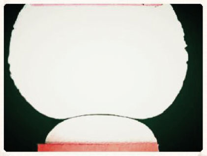
Figure 1. Cross-section image of HiP solder joint.
Most common causes of HiP defect relate to poor wetting or component warpage. Many factors affect solder joint wetting. First, solder is oxidized during reflow.
Lead-free soldering uses higher reflow temperatures, resulting in more solder oxidation during reflow. Second, improper packaging or storage can cause oxidation of the solder ball. HiP defects happen more often with aged components that are not stored properly. Third, flux performance plays a critical role in solder joint wetting and coalescence. During lead-free reflow, solder paste flux is exposed to higher temperatures for a longer time compared with tin-lead soldering. Therefore, lead-free flux should be more temperature-resistant and perform better than traditional tin-lead flux.
In the beginning of lead-free solder implementation, poor flux performance was associated with many solder defects. It resulted in insufficient wetting and was thought the main cause of HiP solder joints. Today, component warpage is shown to have a strong correlation to HiP defects. Indeed, it is one of the most significant factors that can cause head-in-pillow. For years, coplanarity has been used to indicate component warpage that is only accurate at room temperature. Coplanarity is defined as the distance between the highest point and lowest point of the component. However, dynamic component warpage is tied to head-in-pillow and merits in-depth discussion.
Component flatness varies depending on the temperature, and thus, component warpage varies throughout the reflow process. In the beginning of a reflow process, it appears solder balls are initially in contact with the solder paste after placement (FIGURE 2a). Due to the dynamic warpage of the component, a gap between the component sphere and solder paste was created during the soak or reflow time (FIGURE 2b and 2c). During the separation, most of the paste flux was exhausted, and oxidation occurs at the surface of the component sphere and at the surface of the solder at the PCB pad. As reflow continues, the component solder ball at one point is again in contact with the solder from the solder paste. After all, the remaining flux from the solder paste is not active enough at this time to break the oxidation film at the solder surface and results in a non-wetted HiP solder joint. The solder ball just sits on the solder at the PCB pad. The mechanism of head-in-pillow failure is shown in Figure 2.
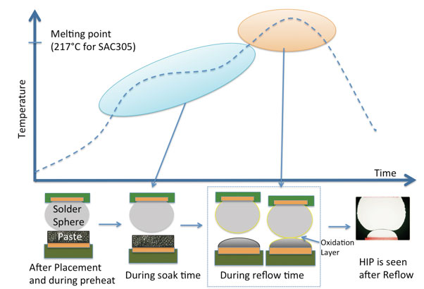
Figure 2. Head-in-pillow defect failure mechanism.
Therefore, a head-in-pillow solder joint is typically seen at the corner pins or at the outer rows of the component where warpage most often occurs. The defect can be amplified when the component is not properly placed and misaligned. Air reflow atmosphere promotes more oxidation and can worsen the situation.
Detection. HiP defects at the outer rows of a BGA can be detected through visual or x-ray inspection. When HiP occurs at the inner rows of a BGA, x-ray inspection is typically used. X-ray inspection for HiP has several limitations. When manual x-ray inspection is used for HiP, detection of the solder joint defect depends heavily on the operator’s interpretation of the images. Also, this is a time-consuming process. When automatic x-ray inspection (AXI) is used, false calls or escapes can happen. FIGURE 3 shows an example of a 2D x-ray image of an HiP solder joint.
Head-in-pillow can be a hidden defect that can escape visual and x-ray inspection during assembly. In many cases, the HiP solder joint still has an electrical connection and is not detected by functional testing. The defect is exaggerated after the component is exposed to some thermal or mechanical stress in the field and causes product failure and field return. Besides, the defect rate of HiP is relatively low, and HiP occurs randomly at different components and pin locations. These make it difficult to diagnose HiP defects.
HiP Mitigation
HiP typically occurs at the corners or outer rows of a BGA. One design approach to mitigate HiP is to enlarge the corner pads or the outer pads of the component where HiP occurs. A larger pad results in more solder deposited at that pad. This design helps increase the chance of solder contact during reflow and results in proper soldering at the (potential) HiP location.
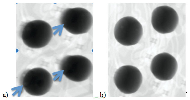
Figure 3. a) 2D x-ray image of HiP solder joints; b) image of normal solder joints.
Similarly, a stencil design can be modified so that more solder is added at the locations where HiP is likely to occur. More solder can be achieved by overprinting the paste on the PCB pad or increasing stencil thickness. More or thicker paste reduces the gap between the component sphere and paste during reflow. It also adds more flux from the solder paste to cope with the oxidation at the solder surface. EMS companies commonly use stencil design modification to mitigate risk of HiP defect during assembly. This approach doesn’t require changes to the pad design, and can be cost-effective compared to modified pad design.
Overprinting the solder paste or enlarging the solder pad will bring the potential risk of solder bridging. When these approaches are used for HiP mitigation, the effectiveness of design modification will depend on the warpage between the BGA component and PCB.
Different solder paste materials have different flux chemistries in their ingredients. Some materials are designed to cope with HiP defect better than others. In general, a paste that helps reduce HiP has the following characteristics:
- Higher print height/volume and consistent volume repeatability.
- Survives a long soak profile and higher reflow temperature.
- Fast wetting speed and good
- wettability.
Good adhesion to the component sphere and good elasticity during reflow. In other words, the paste should be tacky enough to stay in contact with the component sphere during reflow, when warpage happens.
Solder paste materials can be evaluated for their effectiveness of mitigating HiP defect. The solder paste evaluation methodology and its HiP results were published by Nguyen et al1.
Process mitigation. Reflow profiles can be adjusted to mitigate the effect of HiP. In general, in cases of HiP issues, a short preheat (ramp profile) should be used instead of a long soak profile. Reducing soak time will reduce solder oxidation before reflow time (time above liquidus temperature) and cause less flux to be exhausted. Besides, the reflow peak temperature should be as low as possible because more warpage and flux deterioration are seen at higher temperatures. In addition, reflow time should be increased to permit more contact time between the component ball and solder paste and to promote complete coalescence of the solder during reflow. Finally, use of nitrogen will reduce oxidation during reflow, increase wetting and help to mitigate HiP.
The printing process is critical to the success of surface mount component assembly. For HiP mitigation, printing parameters should be optimized for more paste volume and less variation at the suspected locations. Improper component placement or component misalignment can amplify the defect. Inspections should be made to make sure the component is placed properly in the solder paste.
Sometimes, excessive flux is used to mitigate HiP at known locations by dipping the component in tacky flux before placement. This makes more flux available during reflow and helps break the oxidation layer at the solder surface and form a good solder joint. When this technique is used, it is recommended the tacky flux be the same as the paste flux, or at least compatible with the paste flux, to prevent the risk of flux compatibility and other reliability issues. This method is not commonly used because it adds an extra process step and cost to the assembly.
Component Warpage Tolerance
Head-in-pillow defect can be mitigated by solder paste material, pad or paste aperture design, or by optimizing process parameters. However, the dynamic component warpage is the other root cause of the defect that needs to be addressed. Current industry standards on warpage control are insufficient to prevent HiP defect in many cases. This is because the common measurement of component warpage or coplanarity is performed at room temperature, while the dynamic component warpage behaves differently at the actual reflow temperature. There is no good correlation between JEDEC specifications for coplanarity and dynamic warpage at reflow temperature2. High coplanarity does not always create HiP, and low coplanarity may result in head-in-pillow.2,3 There is a change in component warpage from room temperature to higher temperatures, especially for thin packages. Therefore, during the investigation and mitigation of HiP defect, the dynamic component warpage at different reflow temperatures should be measured by thermal shadow moiré or similar technique.
There is no industry standard or criteria on what maximum dynamic component warpage should be for HiP elimination. Although, there is a proposal for this number.3 In general, the recommended maximum dynamic component warpage during reflow should be <3.5 mils for components with 0.8mm pitch and greater when a 5 or 6 mils-thick stencil is used. When a thinner stencil or finer-pitch component is used, the recommended component warpage should be less than 3 mils.
Conclusion
Mitigation of HiP can be a challenge because the defect occurs in low frequency, and it’s difficult to inspect an HiP solder joint. However, head-in-pillow can be mitigated by using good solder paste materials, by modifying PCB pad or stencil design, and optimizing printing and reflow profiles. Different solutions may need to be combined to eliminate HiP. Component warpage is the common root cause of head-in-pillow. When HiP is a concern, the dynamic component warpage should be measured and controlled.
References
1. Jennifer Nguyen, et al, “Evaluation of Lead Free Solder Paste Materials for PCBA,” IPC Apex Expo Proceedings, March 2011.
2. Paramjeet Gill, et al, “Defining Package Warpage Criteria to Mitigate Head and Pillow Defects,” SMTA International Proceedings, October 2011.
3. Alex Chan, et al, “Collaboration between OEM and EMS to Combat Head on Pillowing Defect: Part 2 – Warpage Acceptance Proposal,” International Conference on Soldering and Reliability, May 2013.
is owner of JNK Engineering and Consulting (jnkengineering.com), a provider of engineering services and consultancy in electronics manufacturing. She has years of experience in new technology development, process development and deployment, material evaluation, and PCBA assembly. She also has expertise in design, failure analysis, and reliability. She has researched and published numerous papers on nanotechnology, water-resistant coatings, Pb-free alloys, bottom termination components, Pb-free wave soldering, copper dissolution, no-clean flux reliability, and solder joint reliability. She has led and participated in many consortia projects such as iNEMI and HDPUG. She holds a master’s in electrical engineering and a bachelor’s in chemistry/biochemistry from San Jose State University; jnkengineeringservices@gmail.com.


Press Releases
- Javad EMS Upgrades Through-Hole Soldering Capacity with New SEHO PowerWave System
- Sharpen Your Selective Soldering Skills with Kurtz Ersa's July VERSAFLOW 4/55 Training
- Omron Advances Inspection Technology with NVIDIA Omniverse and Metropolis
- Seika Machinery’s SMI 2026 Webinar Series Continues with Focus on PCB Cleaning Before Solder Paste Printing