Current Issue
Automated Solder Paste Inspection: A New Look at Stencils
What has driven stencil verification to the brink of extinction?
With all the focus on stencil printing to reduce defects and improve profits, electronics assemblers continually invest in custom tooling, new and improved stencil manufacturing methods or materials, high-capability printers, super accurate inspection machines, fancy statistical software and expert training. Ironically, many of the same high-tech assemblers that pour money into ensuring the robustness of their print processes actually skip the simple step of stencil verification upon receipt.
Why has stencil verification become optional and what drove it to the brink of extinction? Likely a combination of efficiency and economics. Basic stencil verification procedures use a negative image of the stencil pattern, a light source and a human to verify the presence of all desired apertures and measure a few of them. As aperture counts increase and sizes decrease, the efficacy of human inspection techniques becomes questionable, and coordinate measurement machines (CMMs) are needed to meet measurement speed and accuracy requirements.
Many assemblers have foisted responsibility for automated inspection and verification onto the stencil vendors, referring to them as “qualified” or “certified” suppliers. In essence, they have placed the fox in charge of the henhouse on a portion of their most critical SMT process. While this practice might look good on paper, it’s rife with potential to backfire and ultimately costs the assembler more money than it saves.
The machines that laser-cut SMT stencils use gantries and motion controls similar to those in pick-and-place machines. Moving parts wear, and machines drift out of spec if they are not regularly maintained and calibrated. The opportunity to create apertures that are out of position, incompletely cut, or obstructed with slag happens every day. And while electroformed foils might eliminate the stencil cutter as a variable, they introduce other factors: their size and positional accuracy are only as good as the artwork used to form them, which depends on the artwork’s photoplotter – another machine full of moving parts. Additionally, the nature of the plating process subjects these foils to regular variations in thickness that introduce error into area ratio estimates.
What’s the probability of getting a stencil with apertures out of spec? Assume the stencil vendor has the highly touted Six Sigma quality in his process. Most are in the sub 5-Sigma range, assuming Six Sigma makes for conservative estimates and easy math. Allowing for the 1.5∑ shift, the supplier creates 3.4 defects per million opportunities. Consider stencils with 10,000 apertures: 100 stencils represent 1,000,000 opportunities. Even at a Six Sigma level, between 3 and 4 of each 100 stencils will have a manufacturing defect. Think about how many stencils are regularly used in production. How many defects are out there right now, waiting to get installed in an assembly printing process?
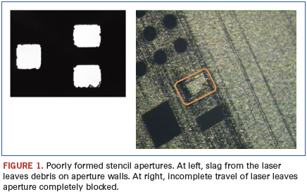
While most stencil manufacturers carefully inspect each piece and verify the quality of their process, mistakes still happen (Figure 1). The ultimate responsibility to make absolutely certain that a stencil is 100% correct before going into production lies with the assembler. But without a CMM to accurately measure the apertures, how can the assembler know for sure? This is where the solder paste inspection (SPI) systems change the game, giving assemblers the tools they need make the final determination of stencil acceptability.
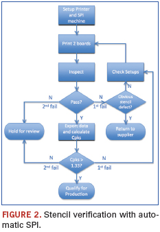
Ray Whittier of Vicor (vicr.com) demonstrates how he uses his white light SPI system to verify new stencils before putting them into production: The official ISO 9001 documented procedure involves printing two dummy boards and inspecting them with the SPI machine. If the machine passes the two prints, the data are exported for further analysis. If the machine fails either print, the stencil is inspected for manufacturing defects. If no obvious defects are found, the machine setups are checked and two more dummy prints are run. If the prints pass on the second try, the data are exported for analysis. If they fail on the second try, the process is stopped and the stencil is held for further review.
The process is flow-charted in Figure 2. The data analysis involves sampling volume readings from the more difficult to print devices, such as SOT883s, SOD882s and µBGAs, as well as for two passive devices, usually 0201s and 0402s. For each component type, Cpks are calculated using control limits of ±50% of theoretical volumes or slightly tighter. All Cpks must be greater than 1.33 for the stencil to be acceptable for production use. If any of the Cpks fall short of the 4-Sigma mark, the machine setups are checked and two more test prints are run. If they again fail to meet the mark, the stencil is held for further review. If the print quality is acceptable, the data are archived and the stencil placed into production.

It takes about 10 min. on the assembly line to get the data, and another 10 min. to crunch the numbers. In addition to being faster and easier than measuring apertures, the SPI method captures process outputs instead of inputs. Where industry used to be limited to measuring the size and position of the aperture and using it as an indicator of a stencil’s performance, we can now measure what really matters: the characteristics of the individual deposits on the PWB. That’s where the rubber meets the road, or, specifically, where the solder paste meets the board.
Au.: SPI systems can be used for a variety of other stencil-related tasks, including vendor qualification, aperture design guideline assessment, and foil material evaluation.
Chrys Shea is founder of Shea Engineering Services (sheaengineering.com); chrys@sheaengineering.com.


