Current Issue
Using Automated SPI to Qualify SMT Stencil Suppliers
Relying on inputs is no longer necessary.
I like to sum up the goal of stencil printing in one simple phrase: Get the right amount of solder paste in the right spot – every time. Any engineer who’s done a stint on a production floor knows that’s much easier said than done. You need the right paste, the right printer setup, the right ambient environment, the right operators and technicians, and the right stencil.
The right stencil starts with the right stencil supplier, but with all the options in metals, manufacturing processes, frame styles, price points and marketing claims, selecting a stencil vendor can be a considerable task, even for a seasoned professional.
Factors in the vendor qualification process should include technological capability, proximity to the assembly house, delivery times, and most of all, quality. While price is sometimes a factor, I personally don’t put a lot of weight on it, because given the influence of a relatively low cost piece of tooling on the high cost of rework, a $50 or $100 difference in purchase price can be recouped in a single shift of defect avoidance.
For years, engineers measured the quality of a stencil by measuring the stencil itself – checking aperture size and location, aperture profile, wall smoothness and foil thickness uniformity. In areas where stencil quality really mattered – the fine features of miniaturized packages – we relied on measuring the input variables of dimensional accuracy. But white light-based solder paste inspection gives us the ability to judge stencil quality based on its actual performance. We can look at the outputs rather than the inputs. And the output – the right amount of paste in the right spot – is what stencil printing is all about.
Empowered with accurate paste volume measurements, we no longer have to painstakingly measure stencil geometry and interpret its influence on process quality. We’ve got a tool that provides hard, irrefutable data on which product provides the best print quality.
When Ray Whittier of Vicor (vicr.com) wanted to choose a vendor, he listed the factors deemed important to his assembly operation, surveyed the supply base, and arrived at a short list of four potential suppliers. He sent artwork to get demo stencils manufactured and began qualification tests. His print operation is fairly challenging because most of his components are miniature ones.
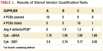
Whittier ran test prints on his NPI line, and used his solder paste inspection system to evaluate print quality. For the tests, he took all the typical precautions to isolate the stencil as the only variable (same paste from same lot, freshly dispensed with four kneads for each stencil, back to front stroke only, dummy boards between test prints, stabilized temperature and humidity, etc.), and measured 10 prints for each stencil. The analysis looked at print yields and at volume repeatability for 0201 and 0.5mm BGA components. Table 1 summarizes the findings.

Supplier A provided the best-performing stencil, which produced 100% yields on the 10-board test and showed the best volume repeatability. Supplier D ran a relatively close second, with similar repeatability, but produced one bad print that contained two defects in the test of 10 prints.
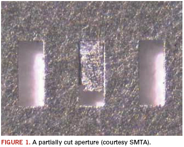
Supplier D was immediately disqualified from contention because the evaluation stencil was missing an aperture. Given that these designs pack about 10,000 apertures in a 4 x 12" area, the missing one could have easily gone unnoticed if the inputs (sample aperture size and location) were measured rather than the outputs (all deposit volumes) of the stencil.
The performance of Supplier B’s stencil was unacceptable: while its volume Cpks were only slightly lower than the others’, its overall print yields were a dismal 50%. It really doesn’t matter that the failed prints only contained one or two bad deposits (a defect rate of 100 to 200 ppm); it takes only one to scrap the entire print.
If only all engineering studies produced such clear and concise data! Whittier’s decision is obvious: Stencils from Supplier A produce the best, most consistent quality prints, making them the primary source. Supplier D is close behind and qualifies as the secondary source. And B and C? Not viable.
By using an SPI to help measure stencil performance, Whitter
1. Identified the best sources for this critical piece of process tooling.
2. Set a performance baseline to which he can compare future stencil performance studies.
3. Increased the level of control on his printing process, and therefore, the probability that he’ll meet his goal of depositing the right amount of solder paste in the right spot more often.
And the best part? The data generation speed: The 10-print stencil characterization test only takes about 20 min. of line time, so it can be accomplished during a product changeover or a lunch break.

Ed.: Due to an editing error, the third paragraph of Chrys’ April 2011 article (p. 44) misstated the aperture sizes. The proper sizes are 0.012”, 0.013” and 0.014”. We regret the errors.
Chrys Shea is founder of Shea Engineering Services (sheaengineering.com); chrys@sheaengineering.com. She wrote this article on behalf of Christopher Associates (christopherweb.com).
Press Releases
- Flying Probe Testing: A Practical Solution for PCB Designs That Traditional Fixtures Cannot Test
- ubersmt Implements PARMI Xceed 3D AOI to Strengthen Inspection and Process Control
- Altus Group Expands Sales Support Function with New Appointment in Ireland
- Kitron Secures EUR 37M order for Next-Generation Tactical Communication Equipment


