

News
News
Compensating for Pb-Free Inspection
Leaded solder joints offer perfect conditions to reflect AOI light beams. How to adjust for Pb-free parts.
The characteristics of a Pb-free joint place higher demands on AOI and the algorithms used. This column describes some considerations required to develop effective AOI algorithms and equipment to test Pb-free assemblies. During development, the algorithms and hardware were tested on a wide range of typical assemblies. Some results are included here.
Most AOI systems feature one or more cameras directed vertically at the test object. Around the cameras are light sources that illuminate the component and solder joint from various directions with different light technologies. The goal of that arrangement is to reflect the light on the solder meniscus’ angle and away from the lens, thus creating significant dark areas for measurement.
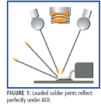
The smooth surface of leaded solder joints offers perfect conditions to reflect light beams. These angular reflections create dark areas in the solder joint’s image that can easily be evaluated by the basic functions of digital image processing (Figure 1). These unique characteristics permit the use of base functions such as a simple gray value analysis (histogram).
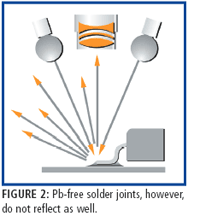
Properly formed Pb-free solder joints have a distinctly pitted surface that reflects light in various directions (scatter). Because light beams are also reflected directly into the camera from the area of the meniscus, a much higher brightness than with Pb-based solder joints is seen (Figure 2). Thus, the measurable difference between a correctly soldered and an open solder joint is smaller.
The optical difference in brightness between a correctly soldered and a faulty Pb-free solder joint is smaller. When using the algorithm described, a higher false call rate or higher failure slack results. Changes due to incidence angle and the light’s spectral structure led to a marginal improvement of the results but it is impossible to attain results comparable to the inspection of Pb-based solder joints.
Changes to the system software to better manage inspection and analysis would reduce the need for major mechanical changes and therefore be more cost-effective for the user.
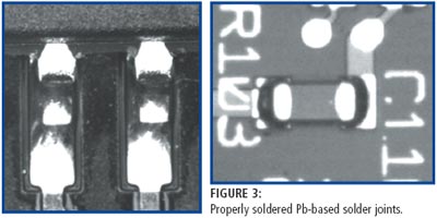
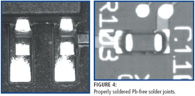
Figures 3 and 4 show representative solder joints of Pb-based and Pb-free soldered assemblies. The increased brightness of the Pb-free solder joints is apparent. To test the PCBs, a program was created by means of the available placement data and optimized by using a leaded assembly. The test program contained 190 components with a total of 748 solder joints. Inspection of solder joints of bipolar components was performed by determining the middle brightness value of the solder meniscus, and by inspection of gullwing solder joints via a new novel algorithm.
When the Pb-based assembly was tested, the only failures were the result of actual component placement errors. False calls did not occur. Testing of a Pb-free PCB with the same parameter settings resulted in the rejection of 18 solder joints, which were exclusively solder joints at bipolar components. That means that the use of the brightness value as the only evaluation criteria causes a higher false call rate. The evaluation by means of the novel algorithm (used for the inspection of gullwing leads) did not cause additional false calls compared to a PCB with a Pb-based solder joint.
The test program was then converted to use test functions similar to those in the test of gullwing leads for all solder joints. On average, two solder joints showed tiny differences from standard solder joints when inspected manually and were rejected. By further modifying the parameters, these too were registered as acceptable joints.
Inspection of two more PCB types generated the same results.
Pb-free solder joints create a higher brightness value on the solder meniscus. Testing using only gray value threshold resulted in increased false call rates, which can be improved slightly by adjusting limit values and optical conditions. In contrast, the new algorithm did not require hardware modifications.
Jens Kokott is team manager AOI systems, Goepel Electronic GmbH (goepel.com); j.kokott@goepel.com.


Press Releases
- Adam Ryder appointed as Managing Director of Incap UK
- Metal Etch Services Opens New Motor City Facility to Meet Growing Midwest Demand
- Yamaha surface-mount line powers the future of specialized production at Inter-Company in Netherlands
- Matric Group Becomes the First U.S. Manufacturer to Deploy Panasonic NPM-GH Dual Lane SMT Technology