Area arrays face higher thermal stress, leading to topside ball delamination. A review of the literature, and a novel solution.
Lead-free implementation will present new challenges for design, soldering and quality control. Higher reflow process temperatures will cause greater thermal stress to the PCB substrate and components. The smaller process window between the higher Pb-free alloy melting point and the maximum allowable component temperature will make soldering more difficult. Specific challenges, however, must be considered to guarantee required DPM levels and minimize in-field PCB failures. In particular, the very small solder joints found on flip chips (FCs) and chip-scale packages (CSPs) will see a great deal more thermal stress during Pb-free soldering, which can result in fatal defects.
This article looks at the existing problem of topside ball delamination for area array packages (FCs and CSPs) by highlighting recent research. The research shown presents important failure analysis data relating to FC and CSP reliability in tin-lead and Pb-free soldering processes. Finally, it introduces an optical inspection technology designed to detect such defects in a nondestructive manner.
Internal designs of FCs and CSPs vary greatly from manufacturer to manufacturer as can be seen in Figures 1 and 2. The extremely small component-side joints of an FC or CSP are at greater risk of failing under mechanical stress. Nakamura and Gu have conducted extensive research1 aimed at understanding the failure mechanism by identifying likely fracture modes and potential delamination sites in flip-chip packages. Their paper “Mechanical Behaviors of Flip-Chip Packaging” clearly shows that the upper solder connection is at greater risk of delamination (Figures 3 and 4).1
 |
| Figure 1: Flip chip. |
 |
| Figure 2: Chip-scale package. |
 |
| Figure 3: Cell analysis - possible failure interface 1: red color indicates maximum stress area.1 |
 |
| Figure 4: Cell analysis -possible failure interface 2: dark color indicates maximum stress area.1 |
Murtuza Rampurawala et al call attention to the problem of topside ball delamination of CSP joints: “Cross-sectional analysis of failed assemblies found cracks within the solder joint along the component side of the assembly.” 2 Figure 5 shows an image of a non-underfilled sample of Package H that failed in torsional testing. The crack initiated from the interface of the solder mask and the pad of the component. Figure 6 shows a cross-section of Package D, underfilled using UF1, which failed after 1825 torsion cycles.
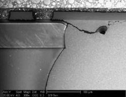 |
| Figure 5: Failed non-underfilled assembly of package H.2 |
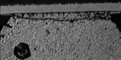 |
| Figure 6: Cross-section of failed package D assembly (UF1).2 |
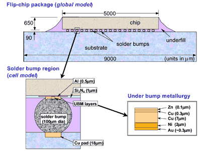
Underfill is used for FCs and some CSPs in order to mechanically strengthen the joint after soldering. If delamination occurs before the underfill process and is not detected, this will cause an early in-field failure. Many area array packages to include CSPs, use an interposer which compensates for the internal tension in a solder joint which is created by coefficient of thermal expansion mismatch during heating and cooling. The general problem with CTE mismatch is illustrated in Figure 7: Due to the fact that the CTE from the PCB substrate and the component body (e.g., 18 ppm/°C for FR-4 and 2.8 ppm/°C for the Si chip2) are not the same, there is a relative movement differential between the expanding materials which increases at higher process temperatures. During cooling, the relative movement differential between the contracting materials can cause a shearing when the solder ball solidifies.
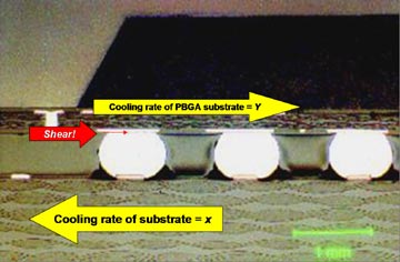 |
| Figure 7: Cross-section of BGA revealing shearing zone caused by CTE mismatch during cooling. |
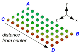
Figure 8 addresses the fact that this movement is greater at the corners of the component. Considering the component from the center outward, the relative movement at the center ball is “0.” Toward the corners of the package, the relative movement differential increases as the distance from the center point increases. The differential is greater at Ball 6 (DX6), for example, than at Ball 3 (DX3). During cooling the materials contract and the relative movement between PCB and component is impeded by solidification of the solder. As all materials will assume their original position at room temperature, a residual sheer stress will remain in the solder joint. This stress is substantially larger at the corners of the component and can result in micro crack formation. For this reason, it is essential that PCB design engineers choose the right material combinations with respect to CTE mismatch.
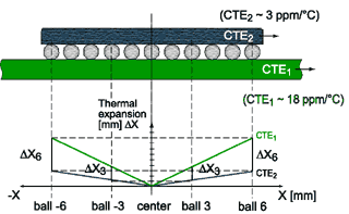 |
| Figure 8: The corner balls are at greater risk of delamination caused by CTE mismatch. |
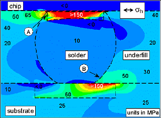
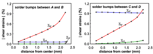
Gu and Nakamura underscore this issue of increased stress at the corners of the package.3 Figure 9 reveals increasing shear strain from the center to the edge, and shows that out-of-plane shear strain is larger near the edges of the component.
 |
| Figure 9: Increased shear strain at corner balls.3 |
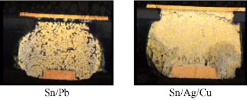
This analysis of the problems of increased corner ball stress as it relates to area array packages, especially in a Pb-free process, is clearly supported by HDPUG’s research: “It can be seen that due to the higher lead-free reflow temperatures, the package is warped severely, leading to the anomalous-shape solder joints near the corner and fatter than normal shape solder joints near the middle. The failure locations of the solder joints of the package are near the corners of the outer, inner, and the thermal ball arrays. This is due to the global thermal expansion mismatch between the package (silicon chip, molding compound, and BT [bismaleimide triazene] substrate) and the PCB, and the local thermal expansion mismatch between the silicon chip, the BT substrate, and the molding compound.” 4 (See Figures 10 and 11.)
 |
| Figure 10: SnPb solder balled 208 PBGA with SnAgCu solder paste on NiAu PCB (no fracture yet). |
 |
| Figure 11: Failed SnPb solder balled 388 PBGA with SnAgCu solder on OSP PCB (at corner of an outer row of solder joints). |
Increased Solder Risk
The basic problems associated with FC and CSP solder joints are amplified in a Pb-free process due to three essential factors: a) the process temperatures for Pb-free is higher, b) the temperature that a Pb-free solder joint solidifies is much higher and closer to the peak reflow temperature than with SnPb and c) the effects of CTE mismatch are amplified at higher temperatures. Figure 12 identifies the problems in more detail.
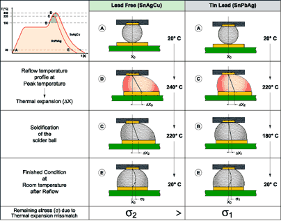 |
| Figure 12: Problems of FC and CSP Pb-free solder joints. |
The startup condition in both processes is the same at room temperature (A). As the assembly heats up in a reflow process, the relative expansion differential (DX3) in a Pb-free process is greater at the higher peak temperature (D), than the relative expansion (DX2) in a SnPb process at its peak temperature (C). At position (C) in the temperature profile, the Pb-free alloy solidifies at position DX2, whereas the SnPb alloy is at its peak temperature. Therefore, during cooling, the contraction of the materials in the SnPb process takes place longer in a fluid or flexible state, and can move back to position (DX1) at the ball solidification point (B). When all materials move back to their original positions (X0) at room temperature (E), the remaining stress (s2) in the Pb-free solder joint is greater than (s1) in the SnPb solder joint. It should be understood that the remaining stress (s) can result in a shearing or delamination even during the first production reflow cycle. Proper inspection techniques should allow for the discovery and correction of such defects before they become costly in-field failures.
Syed underscores the topside delamination problem as it relates to the Pb-free process: “The failures reported above were analyzed with dye and pry and cross-sectioning techniques. Overall, it was found that solder joint failure for all of these Pb free alloys occur at the package side of the joint as is the case for Sn/Pb alloy.” 5 A representative cross-section of joints with SnPb and SnAgCu alloys is shown in Figure 13.
 |
| Figure 13: Cracked solder joints for SnPb and SnAgCu alloys due to temperature cycling. |
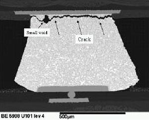
More recently, Syed further underscores this problem: “In all cases reported here, the solder joints failed at package interface. Figure 14 shows a typical cross-section of failed joint showing crack very close to intermetallic on package side.” 6
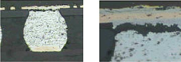 |
| Figure 14: Typical failed SnAgCu solder joint cross-section. |
In summary, given the CTE mismatch problems and considering that corner joints of an area array package have greater stress, it is clear that the Pb-free process for FCs and CSPs will realize a much greater danger for topside ball delamination. The research noted highlights the problems associated with component-side delamination on a variety of FC and CSP devices. Greater care must be taken, therefore, during both PCB design and production to minimize this problem. Most important, however, first-article inspection procedures must be implemented to discover these fatal errors before they result in in-field failures.
Inspection equipment must permit the nondestructive discovery of such defects. Area array packages in general, and FC and CSP packages in particular, have presented great challenges for inspection equipment. The problem lies in the fact that the solder connections are extremely small and hidden under the package. Cross-sectioning of such devices is time-consuming and expensive but can offer the necessary failure analysis information to understand and correct process or material problems. This destructive method, however, cannot be used on all PCBs. In the past 10 years, as area array packages have become an SMD of choice, manufacturers have been using x-ray technology for nondestructive inspection purposes both in and off line. X-ray has proven its usefulness in the discovery of the typical problems such as voids, misalignments, opens and shorts. Also, its effectiveness is improving, particularly in terms of magnification and resolution. Three factors, however, can make this technology at times somewhat limiting: proper interpretation of the image data; the ability to “see” particular defects, such as delamination in the form of micro cracks; the cost of high-end equipment.
The specific problem of topside ball delamination of Pb-free FC and CSP solder joints can present difficulties for even the best 3-D x-ray equipment. Since its introduction to the market in 1999, manual BGA optical inspection equipment has become a state-of-the-art supplement to offline x-ray systems. Until now, it was limited in that the optical system could inspect only the bottom-side joint of low-profile packages such as µBGAs, FCs and CSPs. In other words, the acute problem of topside ball delamination of FCs and CSPs could not be properly inspected by existing BGA optical inspection systems. The introduction of a newly designed flip chip optical inspection system makes the visual inspection of the critical defect area possible, and is a cost-effective alternative to destructive methods.
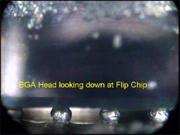
Low-profile CSPs and FCs will require the improved inspection capabilities of a newly engineered flip chip optical head designed for visual inspection. The iris of the original BGA optical inspection system sits approximately 0.30 mm from the surface of the PCB. This provides a “look down image” (Figure 15) of a flip chip whose standoff or gap height is only 0.05 mm. The new flip chip optical head has now lowered the iris to approximately 0.015 mm. It is now possible to “look up” (Figure 16) at even the topside of the flip chip joint to detect possible defects such as topside delamination. This critical topside fillet of FCs and CSPs was not previously seen by BGA optical inspection equipment.
 |
| Figure 15: Standard BGA optics look down at bottom fillet. |
 |
| Figure 16: New FC optics look up at topside fillet. |
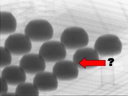
Figures 17, 18 and 19 reveal the importance of this optical innovation by discovering topside fillet delamination of a low profile µBGA. Based on the extremely low iris, the new flip chip optic (Figure 18) permits even the inspection of interior topside fillet problems in the middle of the component, as seen in Figures 20 and 21, which were taken from the same µBGA (Figure 17).
 |
| Figure 17: A µBGA. |
 |
| Figure 18: New flip chip optical head. |
 |
| Figure 19: Corner ball of BGA delaminated. |
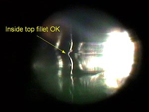 |
| Figure 20: Interior topside fillet OK. |
 |
| Figure 21: Interior topside fillet deformed. |
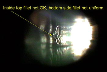
The optical inspection system has successfully been used to discover critical defects in Pb-free CSP production. The topside fillets of a low profile, Pb-free CSP seen below reveals that the middle ball in Figure 22 has a proper topside fillet, whereas the left side corner ball in Figure 23 shows obvious delamination.
 |
| Figure 22: Interior topside fillet OK. |
 |
| Figure 23: Interior topside fillet delaminated. |
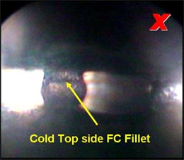
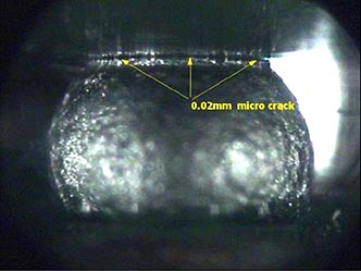
X-ray inspection is state-of-the-art and a necessary technology for nondestructive inspection of PCBs. The particular defect of topside delamination, however, is very difficult or impossible to detect with x-ray technology. Figure 24 was taken with the new flip chip optic, whereas Figure 25 was taken with a state-of-the-art x-ray. These images show that the x-ray alone was not capable of discovering this topside delamination, which resulted in a 0.02 mm micro crack on the Pb-free µBGA. The use of an optical inspection system which can compliment x-ray, especially in a Pb-free environment, should be considered as a sensible requirement.
 |
| Figure 24: Topside delamination visible using flip chip optical head. |
 |
| Figure 25: Using x-ray, the same defect is difficult to detect. |
Conclusion
This article highlights a very specific defect of component-side ball delamination of area array packages, in particular FCs and CSPs, by examining and summarizing current research available on this critical subject. It has become clear that Pb-free soldering will create new process challenges for these components. Simply put, the existing problem of component side delamination will be exacerbated in a Pb-free process. It is imperative to implement proper inspection and test procedures to guarantee a quality Pb-free FC and CSP soldering process. Failure to discover fatal process defects will result in in-field failures, and will generate unnecessary warranty and repair costs. PCB manufacturers implementing Pb-free and using low profile area array packages such as FCs and CSPs should consider using new optical inspection technologies designed to detect these defects in a nondestructive manner as a supplement to their current equipment. The implementation of thorough first-article inspection procedures with newly designed inspection equipment is a cost-effective alternative to destructive methods (or worse, fatal defects).
References
- Toshio Nakamura and Gary Yu Gu, “Mechanical Behaviors of Flip-Chip Packaging,” www.geocities.com/garyyugu/flip_chip_pack/filp_chip.htm.
- Murtuza Rampurawala, Michael Meilunas, Arun Gowda and K. Srihari, “Mechanical Reliability of Underfilled CSP Assemblies,” SMTA Pan Pacific Symposium Proceedings, February 2002.
- Yu Gu and Toshio Nakamura, “3D Interfacial Delamination Near Solder Bumps in Flip-Chip Package,” ASME IMECE, November 2001.
- John Lau et al, “HDPUG’s Failure Analysis of High-Density Packages’ Lead-Free Solder Joints,” IPC Apex Proceedings, March 2003.
- Ahmer Syed, “Reliability of Lead-Free Solder Connections for Area-Array Packages,” IPC Apex Proceedings, January 2001.
- Ahmer Syed, “Accumulated Creep Strain and Energy Density Based Thermal Fatigue Life Prediction Models for SnAgCu Solder Joints,” 54th Electronic Components & Technology Conference, June 2004.
Mark Cannon is president and COO and Juergen Friedrich is director, technical communications, ERSA GmbH (ersa.de); mark.cannon@ersa.de.


