

2005 Articles
The Basics of Boundary Scan
This technique permits reuse of test data and cuts costs by eliminating ICT and functional test.
Even though most test engineers feel knowledgeable with the current test technologies, surveys show that there still is a lack of understanding of JTAG (boundary scan). What exactly is boundary scan? Where can it be used? How does boundary scan work? And, most important: What advantages does it have over other test procedures?
Boundary scan is possibly the most resourceful test technique which, similar to in-circuit test (ICT) but without physical contact, detects failure location, sets thousands of test points – including under BGAs – and needs only four lines (Figure 1).
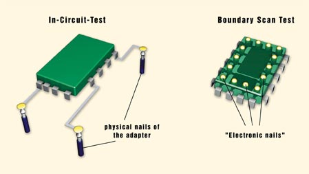 |
| FIGURE 1: Principles of ICT and boundary scan. |
After lengthy discussions about the principles of testing through the stimulation and read-out of integrated thresholds in an IC in the 1980s, boundary scan became a standard (IEEE 1149.1) in 1991. Boundary scan means “testing at the periphery (boundary) of an IC.” Besides the core logic and contact points, some additional logic is implemented in an IC. These test points are integrated between the core logic and the physical pins. All boundary scan cells are combined in a shift register with parallel inputs and outputs and generate the serial scan path.
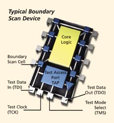 |
| FIGURE 2: Structure of a boundary scan component. |
In each boundary scan IC a control logic, the test access port (TAP), is integrated to stimulate and read-out the cells. The IC is controlled by four signals. Asynchronous actions inside the TAP are executed at the edges of the test clock (TCK) signal, and the TAP’s single states are fixed at each increasing edge, depending on TMS (test mode select). TDI (test data in) and TDO (test data out) represent the input and output of the serial boundary scan shift register (Figure 2).
A boundary scan test can be executed if all boundary scan devices are connected in a scan chain, which has to be placed on the board. Components must be manufactured with these boundary scan cells to be tested effectively by boundary scan test tools. However, if at least one component on the board is boundary scan equipped, it is often possible to (partially) test other components on the boards – such as flash devices. This can be in the case of a cluster test, whereby non-scannable components are connected with boundary scan cells of some boundary scan ICs, and thereby these non-boundary scan components are testable.
Various kinds of tests include:
- Infrastructure test: checks involvement of all scanable ICs in the scan chain.
- Interconnection test: test of all interconnected boundary scan nets.
- RAM test: store test for each possible memory (Figure 3).
- Cluster test: tests scanable and non-scanable components.
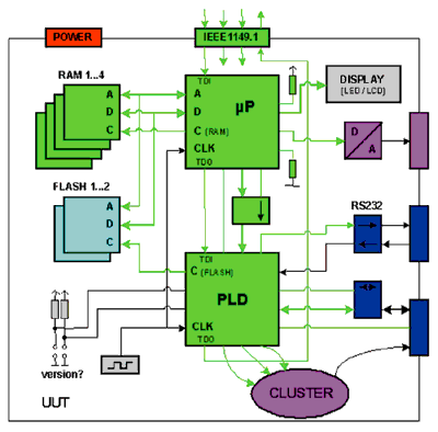 |
| FIGURE 3: Example of boundary scan RAM test. |
Resuable test data. Boundary scan is simple and universally adaptable. In general, the technology supports the product throughout its entire lifecycle. In the design stage, tests are possible by means of CAD data, which also can be used later – even up to the customer’s application. Test patterns created for the design verification can be reused for the prototype debug and fabrication test. This is an important advantage: during the design of highly complex assemblies, testability for the future has to be considered.
Thus, the time and effort required for testing is enormously reduced. Only a few days or even hours are required to generate a test program – much less than ICT or functional test. Furthermore, diagnosis times are minimized, and the (high) production costs of bed-of-nail adapters, which can run into tens of thousands of dollars, eliminated. Tremendous capacities and long storage times for these adapters can also be avoided.
By integrating boundary scan in ATE systems – e.g., fixture-type systems or flying probes – test coverage can be further increased.
Boundary scan’s second field of application is in-system programming (ISP). The programming of PLD and FPGA ICs as well as flash EEPROM ICs play an important role. PLDs and FPGAs are directly controlled by the boundary scan signals TCK, TMS, TDI and TDO. A program can be executed to comply with the respective manufacturer’s conditions.
Flash programming is executed differently because the signals of flash ICs are controlled via boundary scan pins and the write and read accesses are recreated. One big advantage of the ISP process is the avoidance of separate steps in assembly production because it can be tested and programmed in the same environment. Once created, programs can be used again and again. Thus, the expenditure for reprogramming is minimal.
The standardized process enables the automated test set generation with accordant software support, up to the pin level diagnosis. The combination of various boundary scan tests even increases the testability of an object.
Advantages of boundary scan. Using boundary scan accelerates the development of new products. Time is saved in latter stages of PCB production. The test technique also has potential for several cost reductions. The investment required for the purchase of a boundary scan test system is far below the price of a functional tester or ICT. As mentioned, the costs for development, production and storage of bed-of-nails adapters for ICT do not apply. Test program creation via boundary scan can be realized in a significantly shorter time. Diagnosis costs are also reduced as a result of the high test coverage (nearly 100%).
The increasing complexity and I/O connectivity of modern ICs such as PLD, flash and BGA or µBGA microprocessors nearly impedes a physical contact test. The only alternatives are visual inspection by means of x-ray, which costs a lot and comes with certain biases based on apparent health risks, or boundary scan. Because of the direct failure localization, high fault coverage rates can be realized via boundary scan. Also, electric faults can be easily found, an advantage x-ray inspection does not have.
Goodbye, static ICT. Because access problems are growing, the static ICT is going to be replaced by boundary scan technology. Remaining problems such as the recognition of dynamic or analog failures can be covered by a combination of boundary scan with a flying probe or functional tester. For some time there has been discussion over the standard’s use for analog test (IEEE 1149.4). But the number of ICs which support this process is relatively small and the possibility for practical application still in its infancy.
Per IEEE 1149.1 a high quality and mature digital test has been used for years. Boundary scan controllers for all bus systems, for instance PCI, VXI, PXI, PCMCIA, USB or LAN, are available.
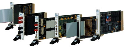 |
| FIGURE 4: Sample boundary scan controllers. |
Hardware and software from low-cost solutions up to high-performance systems are available. Furthermore, a number of additional test tools, e.g., for automated test set generation or coupling with flying probe or functional tester, are available.
Stefan Meissner is with Goepel Electronic (goepel.com); s.meissner@goepel.com.


Press Releases
- Adam Ryder appointed as Managing Director of Incap UK
- Metal Etch Services Opens New Motor City Facility to Meet Growing Midwest Demand
- Yamaha surface-mount line powers the future of specialized production at Inter-Company in Netherlands
- Matric Group Becomes the First U.S. Manufacturer to Deploy Panasonic NPM-GH Dual Lane SMT Technology