

2005 Articles
Stencil Design for Pb-Free SMT Assembly
The new process will require a few tweaks from SnPb standards.
In order to comply with RoHS and WEEE directives, many assemblers are transitioning some or all of their soldering processes from SnPb to Pb-free within the upcoming year. There are no drop-in replacement alloys for SnPb solder, which is driving a fundamental technology change. This change is forcing manufacturers to take a closer look at everything associated with the assembly process: board and component materials, logistics and materials management, solder alloys and processing chemistries, and even soldering methods.
Do not expect a dramatic change in soldering behavior when moving to Pb-free solders. The melting points of the alloys are higher, but at molten temperatures the different alloys show similar behaviors in a number of respects. Expect subtler changes, especially near the edges of a process window that is assumed based on SnPb experience rather than defined through Pb-free experimentation. These small changes, many of them yet to be identified and understood, will manifest themselves with lower assembly yields. The key to keeping yields up during the transition to Pb-free is quickly learning what and where the subtle distinctions are, and tuning the process to accommodate them.
The lower spread of Pb-free solder is a well documented behavioral difference that will require some adjustment. In the particular study described below, the investigators were concerned by the lower spread of Pb-free alloys, especially on organic solderability preservative (OSP) surface finishes. In the world of SnPb soldering, it is a common practice to design stencil apertures that are slightly smaller than their mating pads. If the entire pad is not covered with paste, that’s OK – it will most likely spread over the pad during reflow. In the world of Pb-free soldering the alloy most likely will not spread to cover the pad, leaving some of the copper pad exposed in the final assembly. Figure 1 illustrates differences between the alloys on 0603 and 0805 pads.
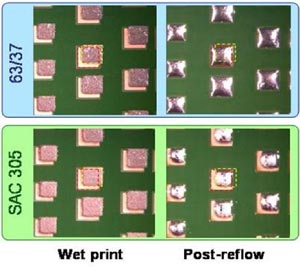 FIGURE 1:
Photos of 0603 and 0805 solder paste prints intentionally offset to
illustrate the lower spread properties of Pb-free solder alloys. Note
that the SAC305 alloy stays right where it was printed.
FIGURE 1:
Photos of 0603 and 0805 solder paste prints intentionally offset to
illustrate the lower spread properties of Pb-free solder alloys. Note
that the SAC305 alloy stays right where it was printed. |
Granted, exposed copper is purely a cosmetic concern and has not been shown to adversely affect reliability, but it is still a concern for many assemblers and their customers. The practice of cropping stencil apertures is used not only to improve fine-pitch print yields, but also to limit the amount of solder deposited onto the pads of passive components. Limiting the amount of paste helps minimize mid-chip solder ball and tombstone defects. If a current aperture design cannot be successfully downsized to limit quality problems without creating new cosmetic concerns, new aperture designs must be developed that address both areas.
The investigators of this study set out to benchmark current stencil design performance and identify optimized aperture designs for Pb-free solder pastes. Baseline data were generated using the known best and worst performing SnPb stencil designs. They then introduced three new aperture designs, identified the best performer, and did some further investigation to verify its merit.
The Investigation
The aperture design study was undertaken in two portions. The first portion benchmarked the performance of aperture designs known to be the best and worst cases for the formation of mid-chip solder balls (MCSBs) in SnPb soldering. These designs were built with both SnPb and Pb-free solder pastes. The second portion sought to improve upon the original apertures’ performance, using Pb-free paste only.
The test vehicle in this study had 100 IPC-recommended pad stacks for 1206, 0805, 0603 and 0402 devices, for a total of 400 devices per assembly. Fifty of each device were mounted horizontally; 50 were mounted vertically. The experimental design in both portions was a full factorial with three replicates. There were a total of 1200 data points per condition set.
The factors in Part I included:
- Solder type – SnPb or SAC305.
- Profile type – ramp or soak (Figure 2).
- Surface finish – OSP, ENIG, immersion silver (ImAg) or immersion tin (ImSn).
- Stencil aperture designs (Figure 3) – benchmarked best and worst cases.
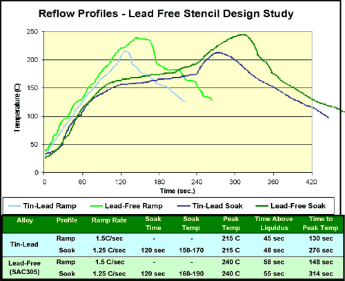 FIGURE 2: Profiles used in Parts 1 and 2 of the study.
 |
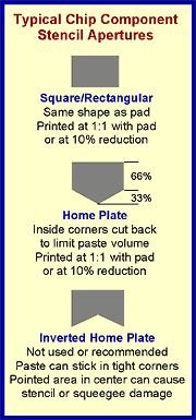 FIGURE 3: Typical stencil apertures. Rectangular and home plate were used in Part I of the study.
 |
The best case was a “home plate” design with the aperture area reduced by 10% on a 0.005" foil. The worst case was a rectangular apertures at 1:1 with the pad on a 0.006" foil.
While the overall average number of MCSBs in Part I averaged 32.6 per board, equating to a device yield of only 91%, the vast majority of MCSBs were produced with the worst-case stencil design. The best-case stencil design averaged only 2.67 MCSBs per board, or a device yield of 99%.
The main effects plot (Figure 4) shows other interesting effects:
- Pb-free solder paste shows far less propensity to form MCSBs than SnPb.
- As expected, the ramp profile produced less solder MCSBs than the soak profile.
- Although the magnitude of the effect surface finish was not as great on the formation of MCSBs as other factors like alloy type and stencil design, the effect was still significant. Immersion tin finishes produced the least amount of MCSBs, while OSP and immersion silver produced more. ENIG produced an average amount of MCSBs.
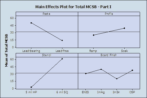 FIGURE 4: Main effects plot for Part 1. Note the decrease in MCSB with Pb-free solder paste.
 |
The factors used in Part II of the study included:
- Profile type – ramp or soak.
- Surface finish – OSP or ImSn.
- Stencil thickness – 0.005" or 0.006" foil.
- Stencil aperture shape – three experimental designs developed through a previous series of screening experiments. The three apertures are shown in Figure 5.
- Radiused home plate.
- Radiused inverted home plate with proportions 20%-60%-20%.
- Radiused inverted home plate with proportions 30%-40%-30%.
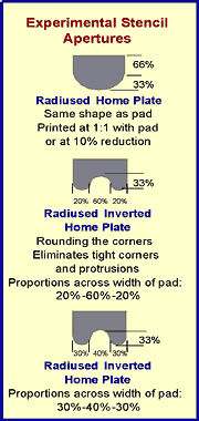 FIGURE 5: Experimental aperture designs
 |
All experimental apertures were at 1:1 proportions with the pads in order to limit exposed copper at the edges.
The average number of MCSBs produced per board was 6.5, or a device yield of 98%. Observations from Figure 6 include:
- Aperture shape has far more influence on MCSB formation than foil thickness.
- The effect of profile type is approximately equivalent to that of aperture shape.
- With SAC305 pastes, the immersion tin appeared to produce slightly more MCSBs than OSP surface finishes, but the effect is not severe.
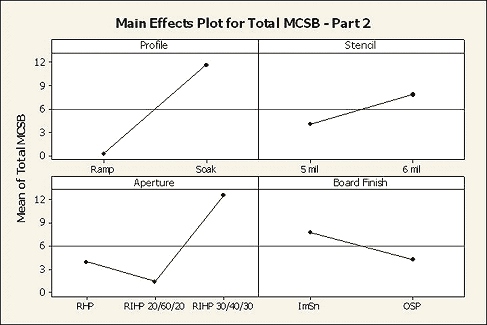 FIGURE 6: Main effects plot for Part 2. Note the dramatic effect of paste volume and profile.
 |
The best aperture identified was the radiused, inverted home plate (RIHP) with aperture proportions 20%-60%-20%. It produced an average of 1.45 MCSBs per board, or a 99.5% device yield. This represents a 45% reduction in MCSBs compared to the previously benchmarked best case of 2.67 MCSBs per board. Note that this average includes the influence of 0.006" foils in its calculation!
Just because an aperture shape remedies one problem, it should not be assumed that it is automatically fit for use. Areas which merited further investigation before the aperture could be recommended include tombstoning, volume and repeatability of the deposits, and spread underneath the component termination.
Tombstoning Performance
Tombstoning has many causes, most of which were not included in this study. But aperture design is a factor in tombstoning, and the investigators wanted to insure that a reduction in MCSBs was not achieved at the cost of increased tombstones.
In Part I, all the tombstone defects occurred with Pb-free solder paste. The effect of the alloy was the clearly the main driver of the results. Tombstoning rates averaged 1.2 defects per board (recall there are 400 devices per board) for SAC305 paste and zero defects per board for SnPb paste. The defect trend of the Pb-free solder alloy followed behavior expected in SnPb systems: it increased substantially with higher solder volumes, particularly when combined with fast ramp profiles. But the SAC305 was far more sensitive to higher solder volumes than the SnPb. This indicates that the Pb-free window is much tighter than the SnPb window with respect to thicker foils and excessive paste deposits as they relate to tombstone defects.
In Part II of the study, the RIHP 20-60-60 aperture shape produced no tombstones. Again, Part II used only Pb-free solder paste, so the defect rate was reduced from 1.2 defects per board to zero defects per board. Insufficient data exist to state that this is an optimum aperture design to minimize tombstoning, but the results indicate a discernable improvement over the two baseline designs. The investigators are planning further studies on tombstoning to characterize its causes in Pb-free systems and with smaller devices.
Interestingly, the RIHP 20-60-20 (known hereafter as simply the “RIHP”) design deposits more solder paste than the homeplate designs used in the study. Depending on the device, a RIHP aperture provides from six to 20% more paste volume when printed with a 0.005" foil and from 20 to 40% more volume when printed with a 0.006" foil.
Although 0402 devices are not particularly difficult to print, they were chosen for volumetric analysis because they were the smallest feature printed in the study. The roughly 3000 in3 deposits have about the same volume as a single 0.020" pitch (QFP208) deposit.
Table 1 shows the average volumes of 400 features, and the standard deviations of the volumes expressed as a percent of the mean. The 0.005" RIHP aperture provided 6% more paste volume and the 0.006" RIHP provided 20% more paste volume – yet neither produced more MCSBs – than the benchmark SnPb aperture design.
TABLE 1: Solder Paste Volumes for 0402 devices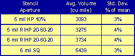 |
The RIHP showed a slightly higher variability in volume consistency than the regular homeplate design. A commonly used rule-of-thumb on print repeatability states that standard deviation should be no more than +/- 10% of the mean volumes. At 3-4%, all four aperture designs showed good volumetric repeatability.
Solder Spread Under Component
X-ray analysis was performed to ensure that the Pb-free solder did spread underneath the components’ bodies to the ends of their terminations. Figure 7 shows an x-ray image of the most challenging spread conditions: a 1206 component (farthest distance to spread), printed with a 0.005" foil (least solder volume) and reflowed under a ramp profile (less opportunity for hot slump).
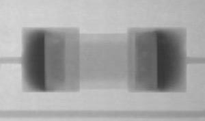 FIGURE 7: X-ray image of 1206 device.
 |
Conclusion
Converting to Pb-free circuit assembly will require some adjustments. The principles and behaviors of solder that are well understood still hold true, but subtle differences in the behavior of the new alloys will call for some fine tuning. The tuning methods will be the same ones used in SnPb soldering for decades: the application of statistical methods, scientific knowledge and common sense.
This Pb-free aperture design study assembled over 67,000 components and produced nearly 3600 solder balls. It was determined that Pb-free pastes are more forgiving than SnPb on MCSBs, but less forgiving on tombstones, where they showed a higher sensitivity to excessive solder volumes.
The stencil aperture that performed best was the radiused inverted home plate (RIHP), which reduced the number of mid-chip balls by nearly half when compared to the home plate design. The RIHP was used successfully in both 0.005" and 0.006" foils, and employs a 1:1 aperture to pad ratio. Further investigation showed that it did not increase incidence of tombstones but did offer more solder volume than the home plate with similar repeatability, and permitted sufficient spread underneath component terminations.
Chrys Shea is manager of R&D applications at Cookson Electronics Assembly Materials (cooksonelectronics.com); cshea@cooksonelectronics.com
SIDEBAR: Quantifying Pb-free Solder SpreadThe commonly employed method of printing a circle of known diameter and measuring its spread after reflow worked very well in the world of SnPb. But with Pb-free alloys, the lower rate of spread, combined with an uneven pattern of the spread, renders this test rather helpless in quantifying or comparing the spread of the alloys on different surface finishes. An alternative solder spread/wetting test involves printing pairs of uniform thickness (0.040") solder paste stripes onto an array of uniform thickness (0.030"), equally spaced traces on the board. The paste stripes have increasing gap sizes between them and are printed in a direction perpendicular to that of the traces, as shown below.
During reflow the molten solder expands along the metal lines on the board. If there is enough spread, the gap between two adjacent solder spots is bridged. The gaps between solder paste stripes are varied from 0.1 mm to 0.8 mm.
There are a maximum number of 20 bridges possible for each gap size. The number of gaps to bridge is counted and the results are plotted as a function of the gap size. The results are shown in Figures A1 to A3.
|
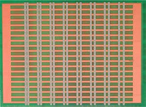
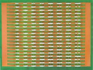
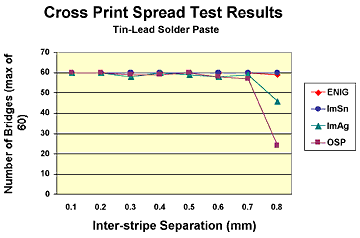 FIGURE A1: Cross print test showing the number of bridges formed by Pb-bearing paste printed on four different board finishes.
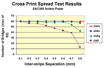 FIGURE A2: Cross print test showing the number of bridges formed by Pb-free paste printed on four different board finishes.
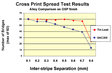 FIGURE A3: Difference in spread of Pb-free and lead-bearing pastes in OSP surface finish as observed in the cross print pattern test.


Press Releases
- Javad EMS Upgrades Through-Hole Soldering Capacity with New SEHO PowerWave System
- Sharpen Your Selective Soldering Skills with Kurtz Ersa's July VERSAFLOW 4/55 Training
- Omron Advances Inspection Technology with NVIDIA Omniverse and Metropolis
- Seika Machinery’s SMI 2026 Webinar Series Continues with Focus on PCB Cleaning Before Solder Paste Printing