

2005 Articles
Poor Vision
The great potential of machine inspection can be undone by poor planning.
The director of purchasing at a major EMS company summarized one of the key issues of automatic optical inspection: “Inspection adds no value in the SMD line ... It does not place parts … It does not reflow parts.”
Coupled with this attitude has been the failure of many AOI systems to meet customer expectations, for a range of reasons. Logic would seem to dictate that a system that can cost as much as a pick-and-place machine should deliver similar value. The initial promise of AOI to improve yields and reduce manufacturing costs was bright, and yet today it provokes much cynicism. Why this has occurred? And how does one gain greater value from an AOI solution?
Automatic optical inspection originated during World War II, when the interpretation of aerial reconnaissance photography meant hours of painstaking inspection of freshly developed film in darkrooms in the Mediterranean and Pacific. Photographs taken from 30' to 20,000' required the interpretation of highly skilled experts to detect gun emplacements, troop movements and ship identification as quickly as possible since thousands of lives were at stake. The first computers were entering use, and were taken up solely for cryptology or weapons development. Thus, simple pattern-matching overlays and optical comparators allowed users to eliminate much of the clutter and focus on what was important. This evolved into simple computer algorithms, most of which continued to develop for intelligence applications. During the Space Age, the first reconnaissance satellites used more sophisticated versions of these algorithms to achieve the same goals. The first AOI systems for inspection of PCBs were based on these technologies, and today’s systems are their evolutionary cousins.
As AOI is widely used in a number of industries and applications, many of the technologies associated with it are better suited to different applications. A misprint on a pharmaceutical label may look similar to that on a component, but the way it is identified and reported can be entirely different. Most AOI systems in our industry are compromises, and by understanding their limitations and capabilities we can better devise a successful inspection strategy. AOI can also be used at multiple locations in the assembly process – on the solder paste printer, after the printer, post-placement and post-reflow – making selection of the best value and performance solution an even greater challenge. One size does not fit all.
Repair costs increase rapidly as value is added to the substrate, making detection and repair at the earliest possible stage the most cost-effective option (Figure 1). While the most widespread use of AOI is probably at the end of the line, detection and repair cost is highest at this point. This will be exacerbated by the higher solder melting temperatures and narrower process window of lead-free. Post-placement AOI has not been as popular because of issues with component movement and the perception that end-of-line is the best point at which to detect all defects. Post-print AOI has also become more popular as system capabilities have improved and the data it amasses (such as the impact of solder volume and shape) become better understood. Best practice engineering dictates the most logical point at which to inspect is the point at which the greatest number of defects can be detected and prevented. The fundamental truth of most AOI technology, however, is that the best it can do is to “inspect defects out” rather than preventing them, which conflicts to an extent with what we have learned from quality gurus such as Deming, Taguchi and Smith (the inventor of Six Sigma).
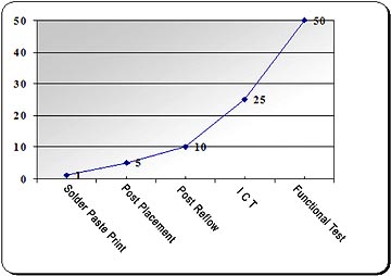 FIGURE 1: The cost of repair rises as an assembly moves through production.
|
The basic goals of AOI are:
- Defect detection – finding all defects except hidden ones and bad components.
- Lowest possible cost to improve and maintain yields.
- Use as a feedback tool for immediate process improvement.
It has been found that a majority (>60%) of defects originate in solder-paste printing (Figure 2).1 While some are self-correcting, many can be fatal. At placement, the most common defects include missing or extra components, misalignment, polarity and wrong component. Post-reflow, this grows to include lifted leads, tombstoning/billboarding and solder-quality defects (Figure 3).
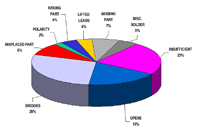 FIGURE 2: A breakdown of defects in SMT processing.
|
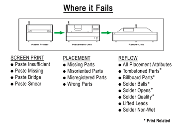 FIGURE 3: Defects can be found throughout the process, but most stem from poor printing.
|
With hundreds of process variables originating at several locations in the process, the demands on AOI can be quite stringent. Understanding the limitations of the technology is critical. Normal process variations such as parts color, fiducial variations, text and markings, substrate color variations and slight positional offset must be accepted without the system flagging them as defects, while true defects must be caught.
7 Pitfalls
Having established the basic requirements and parameters of the technology, the following is a list of issues that have frustrated, foiled and frightened many users to date.
Process responsibility. Responsibility for selection of AOI can be vested in a number of job functions; engineering and quality control departments have input, as does production control, and manufacturing typically has to make it work. This dilution of efforts or splintered responsibility can lead to fingerpointing, acrimony and the horrors of psoriasis and early hair loss.
An AOI implementation strategy is necessary to ensure the requirements and technical considerations of all manufacturing and support functions are considered and answered. A “champion” must assume overall responsibility for successful implementation across all job functions. Consideration of Deming’s 14 points2 for management is an excellent starting point to directly address many of these issues.
Supplier smoke. Perhaps 40 companies worldwide supply AOI systems of one type or another. With such strong competition coupled with a recession only recently ended, many have been desperate to sell as many systems as possible, and some of the performance claims have been hyperbolic at best. The laws of physics are, however, immutable and good engineering, solid performance and support are often self-evident.
In turn, buyers must educate themselves to make a well-informed purchase. The key is to learn from the experience of others and use common sense. As a wise man once said, proper prior planning prevents poor performance.
While pitfalls exist, the opportunity to see real benefit from AOI is profound and directly benefits profitability. Engineering and manufacturing must recognize that every percent improvement in process yields flows directly to the bottom line. AOI offers the necessary direct feedback tool to help meet the imperatives of today’s highly demanding manufacturing environment.
Excessive programming and job setup time. The North American market, with the exception of automotive applications, is primarily high mix, low volume. Production runs of 1,000 pieces or more are uncommon at most facilities. This, combined with aggressive delivery schedules, does not permit long job setups and extensive debugging. Many companies are working on 24 hour deadlines, with kitting, programming of pick-and-place equipment and assembly taking most available man and machine hours. CAM or programming technicians typically program the AOI as a secondary job function, and even the best systems on the market still take two or three hours to program to an acceptable level. While basic programming is relatively straightforward, the devil is in the details. To run a job rapidly, quick programming is essential, and yet to reduce false alarms, extensive debugging is in many cases a must. For example, some AOI systems require 1,000 scans or more to compensate for acceptable image variations when inspecting solder quality. Others require extensive go/no-go programming to achieve the same end. Given the market dynamic, time-intensive setup of production runs is highly problematic.
Training. AOI is a constantly moving target with higher densities, finer pitches and improved performance constantly challenging programmers and operators to push the capabilities of existing hardware. Employee turnover, the challenge to do more with fewer employees and changing end-user requirements all challenge AOI process integrity. However, one of the great issues seen in the field is a lack of ongoing operator/programmer training/retraining programs. Regular software updates and system upgrades would seem to dictate regular review and practice, but constraints of daily production often get in the way.
To illustrate a glaring example, the AOI programmer/operator at one manufacturer left the company and the replacement, who had no training, was able to partially program the system to a very basic level. This became an issue when the company found an inspection cycle time that had previously taken 45 seconds now took 5 minutes per substrate.
Throughput. While related to the above problems, throughput has been a serious issue in implementation of AOI at many companies. High false call rates and poor or difficult programming are the primary causes and can be understood with a simple example.
A 99.5% first-pass yield on a panel with 5,000 terminations still can indicate approximately 25 defects per panel. Each must be verified and inspected. Setting tolerances too widely risks missing critical defects, while setting them too closely increases false calls. Finding a happy medium has been very difficult in many cases, resulting in AOI becoming a choke point in line management.
False calls and escapes. Behavior of the software algorithms and a stable imaging process must deliver simple, consistent and easily understood results. Standard process variations such as substrate/component color, text/marking variations between suppliers and slight variations in reflectivity must be accepted while real defects must be found. In the verification/repair process, if there are too many false calls some will escape. When confronted with perhaps hundreds of similar images, the human eye, even when presented with a high-resolution image, will not detect even some gross defects if it is overwhelmed with similar data and images. Images of solder are notorious for their variations. Thus, gray-scale imaging has been better suited to the application. Even under these circumstances, false alarms result. Color imaging, on the other hand, is much better at finding wrong parts or damaged parts. Detection of defects such as lifted leads, bridging and misregistration is related more to the software algorithms developed by individual suppliers. The greatest frustration seems to result from either missed solder defects or related issues such as lifted leads or under-component defects. AOI cannot effectively look under components with any degree of reliability. Finally, one must devise a process in which the operators and engineers have faith in the results. Otherwise implementation will fail.
Correlation of data to other test and inspection tools. Implementation of AOI has been fractional in most facilities, and most still have a mix of AOI solutions combined with manual inspection and electrical test, primarily in-circuit test (ICT) in North America. Correlation of the results at each stage has been problematic. To maintain a competitive advantage, system architecture purposely does not output data in easily transferable files. Despite this, correlation based upon pin reference designators, “stamp” or component identification is readily achievable.
By tracking defects across each platform, a much better picture of the failure mechanism can be seen. Unfortunately, manpower constraints, differing terminology and system architecture issues combine to make the real goal of inspection and test – process improvement – that much more difficult to achieve. Traceability in military, medical and automotive applications would seem to dictate common formats, but little work has thus far been done in the field. n
References
- R. Durairaj, G.J. Jackson, N.N. Ekere, G. Glinski and C. Bailey, “Correlation of Solder Paste Rheology with Computational Simulations of the Stencil Printing Process,” Soldering and Surface Mount Technology, January 2002.
- W. Edwards Deming, “Out of the Crisis,” 1982.
Matt Holzmann is president of Christopher Group (christopherweb.com); mattholzmann@earthlink.net.


