

2005 Articles
Converting Wave Soldering Equipment to Pb-Free
A pair of approaches for incorporating a low-cost wave solder pot.
Sidebar 1
Manual Pb-free Solder Pot Installation• Wear high temperature protective gear (i.e., thermal insulated safety gloves, safety glasses, apron). • Loosen the bolts on the solder pot and pump assembly. Disconnect the pump conduit from the solder pot box at the connector. • Heat the solder pot to approximately 530°F. Once wave temperature has been reached, turn off the heaters and the wave system. Do not start removing the solder with the heater on! Tag and lock the electrical breaker or safety disconnect switch. • Ladle the SnPb solder alloy from the pot into stainless steel trays or aluminum trays. Disposable aluminum trays are acceptable for this application. Spread the trays on multiple tables. The solder is hot and is heavy. A heavy duty table metal table is ideal. Do not place too much weight on the table. • Using thermal insulated gloves, carefully remove the pump assembly. Two people are required to perform this task. The pump assembly will contain liquid solder so remove the assembly slowly and elevate the front end of the pump assembly so the liquid solder will drain from the pump housing back into the pot. • Once the pump assembly is drained of solder, place it on a metal table and allow it to cool before placing it on a skid for storage. Remove the balance of the solder and place it in a tray for future use or reclamation. When the solder has solidified and cooled, move the trays to a skid for storage. • Disconnect the drive shaft on the solder pot. Disconnect the power connector from the pot. • Remove the pot from the wave soldering system. This will require at least two people due to the weight of the pot. • Install the new Pb-free solder pot. This will require at least two people due to the weight of the pot. • Reconnect the drive shaft on the solder pot. Reload the solder pot with 500 lbs. of bar alloy. • Reconnect the power connector to the pot and the pump conduit to the solder pot box at the connector • Cover all the heating elements with solder. The heating elements can be damaged when exposed to air for extended periods of time at high temperatures. Turn on the solder pot heaters and allow the alloy to melt. • Continue to add solder until the upper heaters are completely covered with liquid solder. Once the top heaters are covered with liquid solder, carefully install the pump assembly into the pot wearing high temperature protective gear. • Heat the pot until it reaches 500°F or the recommended temperature of the Pb-free solder manufacturer. Continue adding solder until the solder level is approximately 0.25" from the top surface of the melting pot. |
|
Sidebar 2
Modular Pb-free Solder Pot Installation• Turn off the power to the solder pot and allow the solder to solidify before removing. • Disconnect the power via a quick connect. • Using the motorized pot drive, via a push button, allow the pot to load onto the rollaway solder pot cart. • Disconnect the drive shaft. • Move the Pb-free pot and cart into load position. • Reconnect the drive shaft and via push button allow the pot to load into the machine. • Reconnect the power via a quick connect electrical connector. • Turn on the power. |
With the introduction of Pb-free solders on the production floor, there have been several questions on converting a SnPb wave soldering process to accommodate a Pb-free solder alloy. Some facilities resign themselves to acquiring a new wave soldering system for Pb-free solder alloys, but that can be costly. The Electronics Manufacturing Productivity Facility (EMPF) faced this dilemma. Instead of purchasing a new system, the facility converted the existing system to accommodate both SnPb and Pb-free solders. It was not as simple as acquiring and installing a new solder pot, the EMPF found.
High Sn content solders can have a devastating effect on traditional solder pots. Sn surface erosion dissolves the base metals typically used to manufacture solder pots (Figure 1). Pb-free solder alloys also dissolve metals often used in soldering fixtures, like aluminum, copper and brass. This surface erosion phenomenon will quickly contaminate the Pb-free solder and affect soldering quality.
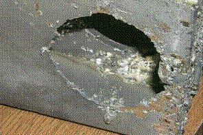 |
| FIGURE 1: Solder pot damaged by tin erosion (courtesy The Welding Institute). |
Technical Devices, a partner of the EMPF, developed a solution for Sn-induced erosion by coating solder pots with a titanium nitride finish. Titanium nitride serves as an effective barrier to Sn. The titanium nitride coating is molecularly bonded to the stainless steel, providing the solder pot and its critical components a protective barrier against the solvent action of Sn. Some of the most critical components in the solder pot and pump assembly are made of pure titanium and then coated with titanium nitride, preventing Sn-induced surface erosion.
There are two ways to remove a solder pot from a wave system and install a new pot. The first procedure assumes that the wave system lacks the convenient quick-disconnect electrical and mechanical connections for the SnPb pot and the Pb-free pot. This procedure may be employed when installing a new Pb-free pot, depending upon the capabilities and flexibility of the wave manufacturer. The approximate time to perform this procedure is eight hours. A typical list of the process steps are in Sidebar 1. (This list is meant to provide an idea of the scope of work. The equipment manufacturer should be consulted for specific details related to the reader’s equipment.)
There is an easier procedure to convert a wave system from SnPb to Pb-free alloys. This assumes that the wave has the quick disconnect electrical and mechanical connections for the SnPb solder pot and the Pb-free solder pot, and is described in Sidebar 2.
This modular approach reduces the time to complete a conversion to less than one hour. As illustrated in Figure 2, this procedure can provide a manufacturer with wave soldering capability for SnPb and Pb-free alloys.
|
|
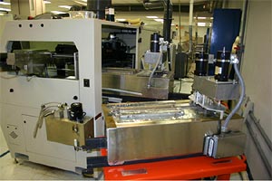 FIGURE 2a: Pb-free and SnPb wave solder pots.
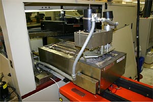 FIGURE 2b: Solder pot installation into wave soldering system.
The EMPF requires SnPb and Pb-free wave soldering capabilities to support process development and prototype manufacturing functions. The EMPF encountered several operational issues when switching from SnPb to Pb-free solder alloys:
- Each solder pot must be labeled, identifying the alloy. This is to ensure that all operators and engineers know which solder alloy is in the pot.
- Remove Pb solder splatter from the rails and fingers and in the pot area. This will prevent the addition of SnPb solder alloy back into the Pb-free solder pot, causing lead contamination.
- Remove all SnPb bar stock from the wave soldering area, to prevent an operator from placing SnPb alloy bar stock into the Pb-free solder pot.
- Place a PB-FREE ONLY sign on the wave system, with the Pb-free solder alloy displayed, and advise everyone in production.
- Clean the finger cleaner as SnPb may accumulate in this system. Pb-free solder alloys have a tendency to stick to the fingers. The finger cleaner on the wave system should remove all solder and flux residues.
- Initially, the EMPF set the solder pot for 500°F, the same temperature as was used for the SnPb alloy. The EMPF observed that the Pb-free solder alloy took 30 to 40 minutes longer to reach its liquid state. In operation, the EMPF determined that the Pb-free solder pot temperature should be set at 509°F, to promote good solder joint wetting and formation.
- The EMPF determined that the dancer and laminar wave height controllers had to be adjusted, to compensate for the density and surface tension differences between SnPb and Pb-free solders.
- If your wave system has an air stone for fluxing PCBs, make sure the flux is recommended by the solder manufacturer. If you choose to use flux not recommended by the solder manufacturer, ensure that it is compatible with your soldering and cleaning processes.
The same SnPb wave soldering process development procedures are in effect for Pb-free alloys. As with SnPb wave soldering, the goal for Pb-free wave soldering is to eliminate the amount of touch-up after the soldering process. A thermal profile will have to be generated, with adjustments made to the preheating zones and the conveyor speed. Performing a wave solder level check ensures complete board coverage during flux application and wave soldering. The prime difference comes from the higher temperatures associated with most Pb-free solder alloys. In the EMPF’s experience, while the solder pot temperatures between SnPb and Pb-free alloys are approximately the same, the Pb-free alloy preheat temperatures are considerably higher – up to 45°C (113°F) – than SnPb preheat temperatures. Due to the higher temperatures, boards and components should be baked prior to production to remove residue moisture.
The EMPF now uses Pb-free alloys in the wave system in its demonstration factory. The Pb-free wave soldering process is being used in ACI’s Pb-free Soldering Training Course and for Pb-free process development, prototype manufacturing and testing. The resulting Pb-free wave solder joints have a grainy appearance, when compared to SnPb. However, it is possible to produce Pb-free wave solder joints similar in appearance to SnPb (Figure 3).
|
|
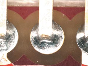
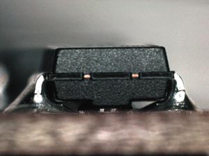 FIGURE 3a and 3b: Pb-free wave solder joints.
The EMPF has used SnCu and SnCuNi solder alloys, but the Pb-free solder pot can be filled with other Pb-free solder alloys such as SnAgCu. Future plans at the EMPF include installing nitrogen to the wave soldering process. This will be a part of a study to quantify how wave soldering in an inert atmosphere will improve process solderability while reducing the amount of solder residues and dross generation. Further information will be available upon this study’s completion. n
Bibliography
- Lead-Free Solder Equipment Damage Workshop; The Welding Institute, May 2002.
Lee Whiteman is senior manufacturing engineer and Jeff Stong is EAD coordinator at American Competitiveness Institute (aciusa.org); lwhiteman@aciusa.org. Debbie Alavezos is technical sales manager at Technical Devices Co.
The American Competitiveness Institute is a scientific research corporation dedicated to the advancement of electronics manufacturing processes and materials for The Department of Defense and industry. Beginning with this issue, ACI will author a regular series on manufacturing.


