

2005 Articles
A Stirring Solution
Intermetallic crystals form more easily in Pb-free solder pots, but there's a fix.
The formation of intermetallics in solder during wave soldering is normal. Intermetallics are seldom found in SnPb solder due to the low rate at which these crystals form with this solder. Pb-free solders cause these crystals to grow much faster; as a result, they can often be found in the solder pot.
As solder comes in contact with wettable metal, some of that metal dissolves into the solder and an intermetallic layer is formed at the surface of the wettable metal. Each wettable metal can to a certain degree be completely dissolved in the solder and will not form an intermetallic below that level. This level depends on the solder alloy, the solder temperature and the metal that is involved; e.g., for copper, this level is about 0.3% at 250°C for eutectic SnPb solder. At higher solder temperatures this level increases, while at lower temperatures it decreases.
If metal is dissolved in the solder beyond the solubility level, this excess will form an intermetallic with the tin in the solder. These intermetallics of copper-tin or iron-tin (the most common) form a hard needle-shaped crystal. These small diameter crystals can be up to several millimeters long and will make the solder more sluggish when entering the solder flow.
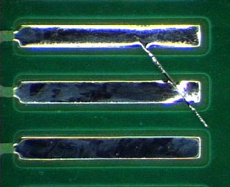 |
| Needle-shaped intermetallic (FeSn2) crystal causing bridging (shorts) in a Pb-free wave soldering process. |
Most of the crystals will collect in the corners of the solder pot where there is almost no solder flow. In such areas, lumps of solder with a high amount of these intermetallics can be found in due time. These lumps are pasty or even almost solid at normal solder temperatures and they should be removed at regular intervals. They can also often be found near the pump area.
If these contaminating lumps are removed at regular intervals, it is not necessary to change the contents of the entire solder pot. The frequency of this maintenance has to be proved by checking the quality of the solder joints. As long as solder process quality is not affected, a slight contamination by intermetallics in the solder is permitted.
Note that solder in the pot is continuously refreshed by the addition of new solder to compensate for solder consumption from the pot. Therefore, it is in most cases not necessary, nor recommended, to drain the solder pot and replace the contents with new solder.
Bridging a possibility. Because higher process temperatures are required for Pb-free wave soldering processes, intermetallic crystal formation is more commonplace than in standard SnPb soldering. Also, the higher tin concentration speeds the dissolution of metals such as copper and iron that are in contact with the molten solder. This is due to the fact that tin is the alloying element. In SnPb solder, the lead does not form an alloy with copper or iron at normal process temperatures. The dissolution process is also affected by the presence of silver in SAC alloys. The silver seems to make the solder more “corrosive” relative to the metals wetted by the solder.
If the lumps of solder/intermetallics are not removed in time, the crystals will be picked up by the solder flow in the pot. These crystals can come to the wave surface and be deposited on the PCB, causing bridging between joints. Removing the contaminated lumps and topping up the solder bath with fresh solder will eliminate this problem in most cases.
Employing a sieving action – stirring solder in the pot slightly with a perforated ladle to pick up the floating crystals – will remove even more of the intermetallic particles. This is recommended if too many crystals are present in the solder flow. The effectiveness of this approach will increase when the solder pot temperature is lowered prior to filtering.
Since most intermetallics will be collected in the “dead” areas, they do not have a direct effect on the process. As long as they do not accumulate in too great a volume and are not part of the solder flow, these contaminated solder lumps will stay put and will not have a detrimental effect on the process. They can only affect the process if they enter the solder wave.
Crystal formation cannot always be avoided if molten solder is in contact with wettable parts of the solder pot. The dissolution rate is still so slow at normal process temperatures (i.e., up to 260°C), there is no risk to the pot material within the typical five-year warranty. Only inserts that are in direct contact with the relatively high solder flow areas may wear out prematurely if not protected with a resistive coating. Even stainless steel will be affected by Pb-free solders if not properly protected.
Gerjan Diepstraten is a senior process engineer with Vitronics Soltec BV (vitronics-soltec.com); gdiepstraten@nl.vitronics-soltec.com. His column appears monthly.


