

2005 Articles
Pb-Free Rework Differences and Practices
No lead means using four heating zones and one cooling zone for reflow.
Pb-free exacerbates issues of time, cost, quality and repeatability associated with rework. Extra time and cost are involved to retrain operators to perform Pb-free assembly, rework and inspection. The cost of Pb-free materials like solder bars, wires and wire core solder is more expensive than eutectic solders. The operating window for Pb-free assembly and rework is considerably smaller and tighter in terms of processing temperatures (approximately 30-35°C), meaning more precision and accuracy are required in profiles and procedures. This also means more research time is needed to investigate and set up proper rework procedures.
Good assembly practice calls for retrained staff and new profiles. Maintaining high quality rework is more challenging because the PCB and components adjacent to the targeted rework component are subjected to multiple cycles of higher temperatures. To maintain the integrity of the PCB laminate, the maximum preheat temperature is set approximately 10°C below the Tg of the PCB material. Higher thermal preheat temperature minimizes the potential thermal distortion and shock to the PCB during reflow. Thick boards – 0.093" or more – require additional heat, have greater �T across assemblies and may require slower reflow oven line speed. As overall board size increases, the process window tends to shrink.
Solder pastes. The rework process is the same no matter the paste. It begins with a good thermal profile, removal of failed components, cleaning and preparing the site, and removing rust or solder residues. Next, the component is replaced with new flux and solder, reflowed and inspected.
Several major differences emerge here between Pb and Pb-free rework. These differences introduce a host of challenges and newer or altered practices. The higher temperatures of Pb-free rework mandate tighter processes, better thermal profiles and greater precision. Otherwise, a number of problems can occur. For example, too much heat could create a blowhole on a BGA ball, but too little heat could lead to BGA balls separating from the PCB substrate. Excessive thermal stress could cause micro-cracks on a BGA and PCB (Figure 1).
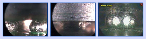 FIGURE 1: A blowhole (left) on a BGA ball caused by excessive heat. BGA balls can separate (center) from the PCB substrate as a result of insufficient heat or the wrong thermal profile. Microcracks (right) on a BGA and PCB are caused by excessive thermal stress.
 |
Hundreds of Pb-free alloys are available. But there is no direct drop-in replacement for SnPb solder; nothing is as effective, costs the same and is nontoxic. Compared with SnPb, every Pb-free replacement alloy is inferior in some cost or performance aspect. Table 1 compares three popular Pb-free solder pastes.
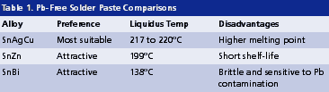
SnAgCu (SAC) alloys are widely regarded as the most suitable choice in the near future for Pb-free soldering. The liquidus temperature of SAC alloys is 217° to 220°C, about 34°C above the melting point of eutectic SnPb. This higher melting range requires peak temperatures in the range of 235° to 245°C to achieve wetting and wicking. Lower peak temperatures (such as 229°C) can be used for SAC solders. Adding copper to SnAg reduces the melting point, improves wetting and increases long-term reliability. Also, SAC is not as sensitive to lead contamination as Bi-containing alloys and can be used with SnPb-plated components with no major problems.
SnZn and SnBi are two attractive alloys due to their low melting points – 199° and 138°C, respectively. SnZn is ideal for soldering to aluminum and its constituent metals are inexpensive. However, zinc reacts with both acids and bases, and as a result, solder paste with this alloy has a very short shelf-life.
The low melting point of SnBi is attractive because there is considerably less thermal shock to the assembly during reflow and less energy is required. But this is a brittle alloy with poor shear strength. Plus, it is sensitive to lead contamination.
Thermal profile. The higher temperatures used for Pb-free processing and rework place greater stress on components and boards, which is further aggravated by cumulative heat exposures. The combined reflow and rework heat cycles can result in a single assembly being exposed to as many as five thermal heat excursions that include two reflow passes, a wave solder pass and two localized heating passes for rework.
The internal package structure within components and PCBs must survive all processes and still provide long-term reliability. Component effects include increased moisture sensitivity levels, thus resulting in shorter exposed floor life, while PCB laminates must minimize internal layer delamination, via cracking and board warpage.
SMT first-pass reflow processing typically has the following characteristics:
- Four-to-six minute cycle times.
- Temperature ranging from 230° to 250°C for joints and body temperatures.
- Delta T ranges from 5° to 20°C on single assembly.
- Time above liquidus ranging from 60 to 90 sec.
The minimized superheat required for Pb-free assembly and rework emphasizes profiling. It is not uncommon to use one profile for a family of assemblies of similar size and complexity. This is usually workable in an SnPb process as it is characterized by a generous process window. Provided the assembly reaches about 200°C, one can be reasonably confident that all components will solder properly. This approach does not work with Pb-free assembly and rework, which requires more precise reflow temperature cycles.
Reflow. Convection – not radiation – is the heating method of choice. Conduction or a soldering iron is not an option. Convection permits tighter process control critical for establishing a sound, repeatable thermal profile. With a good thermal profile, the component will not be overheated or held for too long above reflow.
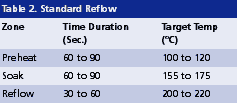
Table 2 shows zones, time durations and target temperatures for standard reflow temperatures. Table 3 shows the same for Pb-free reflow. The higher temperatures, together with the thermal sensitivity of such devices as BGAs and CSPs, present challenges and some ovens lack the capability to ramp temperatures at a rate that will avoid harming these packages. It is vital, therefore, to use four heating zones and one cooling zone, as opposed to the once-conventional three-zone models with no cooldown. Further, the addition of controlled preheating avoids thermal damage to sensitive packages unsuitable for heating above 240°C with quick reflow times.
Some Pb-free reflow profiles are as short as 15 sec. above specified reflow temperature. A typical Pb-free thermal profile can have peak temperatures ranging from 223° to 235°C and may spend only 14 sec. in the reflow zone. This means accurate temperature and profile controls are essential.
To help protect packages from the higher heat of Pb-free processes, use independent top and bottom heater controls. It is a challenge to develop a thermal profile that can reflow the new alloys without damaging CSP and BGA packages.
Through closed-loop, time, temperature and airflow parameters, contemporary rework systems can help operators adapt to Pb-free. Also, enhanced process control features guarantee repeatability. Different voltages and frequencies affect machine performance in many cases.
On any reflow soldering system that heats both sides of an assembly, the required solder joint temperature is a function of how much heat is applied to both sides. While it is possible to reach a specific solder joint temperature with a number of heat settings, the incorrect combination can lead to low yields and in some cases, catastrophic results, including warping due to excess heat on the topside. This often causes bridges in the corners of BGAs and CSPs.
Temperature restrictions imposed by the upper limits of the components mean Pb-free alloys have a smaller reflow process window. Depending on the selected flux chemistry, a window of as little as 10°C may be all that is available. Careful profiling of each assembly thus becomes critical.
The usual rule of good design and the same logical approach to troubleshooting still apply. But beware: two common problems of Pb-free soldering are tombstoning and voiding. Tombstoning is caused by differential wetting across the ends of the component, and used to be common in vapor phase soldering. Unlike SnPb, reduced tombstoning is expected with Pb-free since SAC has a much lower wetting speed than SnPb. However, practical experience shows that tombstoning is more likely. This is attributed to the higher surface tension of the alloy, which has a greater “pulling” force on the component despite the slower wetting speed. With careful profiling and adherence to good design rules, tombstoning can be avoided.
BGAs and CSPs. BGA and CSP rework requires excessive localized heating, increasing the possibility of damaging components with low melting points such as connectors, standoffs or adjacent moisture-sensitive devices. Take care not to overheat any internal thermal grease if the BGA is capped.
Increased voiding is common, especially with BGA and flip-chip components. This is particularly true when SAC paste is used with SnPb-plated components. The peak temperature of 230° to 235°C must be reached to reflow the solder paste. However, component plating is still SnPb, so the plating will endure 50°C of superheat for two minutes or more. Hence, oxidation occurs much more rapidly when the alloy is liquid, and the resulting higher oxide levels cause more voiding. In general, SnPb components with SnPb solder show less voiding than SnPb components with Pb-free solder. Conversely, Pb-free components with Pb-free solder also show less voiding. Careful control of the preheat profile can minimize the size of voids, if not their numbers.
For BGA rework, keep the bottom set point to 50°C or higher, with peak temperatures at 230°C (minimum for joints) to 225°C (maximum for body). Time above liquidus must be between 45 to 90 sec. up to 120 sec. maximum. Thermocouple attachment must have at least two solder joint temperatures and two package body temperatures (center and corner for both).
Trained operators. Trained and experienced operators using new process control practices can play a paramount role in successful rework. If minimal warping occurs, for example, a BGA lifted by just 0.1 mm across the device is enough to cause an open circuit. Even if the board-component interconnection survives this process with no apparent defect, the joint will be constantly under strain as the board returns to its normal shape, causing long-term reliability problems. Eliminating warpage generally involves creating a better balance between the bottom and topside of preheat temperatures. This is best achieved by attaining proper temperature balances in the reflow oven.
If new rework practices and procedures are not implemented, untrained operators will probably apply extra amounts of flux and solder to meet the higher Pb-free temperatures. This increases the possibility of shorting the Pb-free component – and more rework.
Zulki Khan is founder and president of Nexlogic Technologies Inc. (nexlogic.com); zk@nexlogic.com.


