

2005 Articles
Switching to Pb-Free
How difficult is it? Very, says this four-part series on materials, equipment and process considerations.
Soldering is a joining technology employing two base metals and a third metal or alloy to complete the union. In practical terms we usually encounter a bare circuit board and components with their respective metalization joined to make an electrical connection. Other applications range from wire harnesses to connectors and lamps. The basic principle of soldering remains the same, however.
When switching to Pb-free, the product dictates all restrictions. The cost (that is, the retail price) of the product and its reliability enforce certain choices and the parameterization of processes. Examining those details ensures that future product will meet required standards – and hopefully the required price. We start with two important aspects: the PCB and components.
The EU directive concerns PCBs in two ways. The elimination of halogenated flame retardants in the laminate material is a direct effect. Also, because lead is eliminated from the solder alloy, metalized surface finishes and solderability will become considerations. There is also an indirect effect: the impact on process parameters. Moreover, the higher melting point of Pb-free alloys may necessitate more expensive material.
Laminate. Compliance with the first legal condition can only be accomplished by specifying PCBs without the banned halogenated flame-retardants. Direct cooperation with the board manufacturer will be necessary when specifying the laminate material to be free of such additives. Board material that uses other (phosphorous-based) flame-retardants is on the market. Although apparently not as efficient as halogenated materials and suffering from other ills (e.g., absorption and retention of humidity), they do meet the legal constraint. Close cooperation between user and board manufacturer makes sense as the choice of alloy will affect the properties of the board.
Two main choices for Pb-free solder exist: an alloy with a substantially lower melting point than eutectic SnPb or one with a substantially higher melting point. If users decide that relevant restrictions permit use of a bismuth solder, then a few process changes are necessary. The halogenated flame-retardant has to be eliminated from the board material. However, in terms of thermal exposure, the situation is superior to SnPb. Standard FR-4 and FR-3 materials meet temperature constraints as they have for Pb-bearing solder processes.
If, however, a SnAg, SnAgCu or SnCu solder is chosen, much higher temperatures are encountered in the process. Even preheat temperatures (wave and reflow) will rise. In this case, conventional FR-4 will be thermally stressed beyond its capabilities and will have to be replaced by a board that is halogen-retardant-free and that can withstand the heat. Typical glass transition temperature for FR-4 is around 140°C. Laminate Tg will have to rise another 30° to 40°C to minimize thermal damage to the board. For such cases high-temperature FR-4 is offered by a number of suppliers. In this area, standardization is lacking, as actual properties vary greatly from supplier to supplier.
Soldermask. Soldermask has its share of problems even under Pb-bearing soldering conditions, especially during wave soldering. Solder balling (or beading) is just one of these predicaments. If we raise the temperature, we may come to the end of its useful range. No better material seems to be coming. Until improved material is available, a mid-term solution may be a more controlled application and curing polymerization) of the substance.
Surface finishes. For most applications, Pb-free does not always means free of lead. In those cases, any coating on the PCB cannot contain lead. Several studies have shown1 that even minor traces of lead in the joint cause low melting phases. (Some investigators also have tied lead in the metalized coating to the phenomenon of fillet lifting, but the actual cause is still under discussion.) Low melting phases are when areas within the joint have (eutectic) pockets of alloys that melt at substantially lower temperatures than the Pb-free solder used. Such pockets lower the reliability of the joint, particularly its resistance at elevated temperatures during use, and thus are not acceptable. It is important to understand that for some solders, such as SnAgCu, small amounts of lead may be acceptable. It is not yet clear how the limits for trace amounts can be defined safely. Furthermore, obvious differences between wave and reflow soldering exist.
A number of alternative surface finishes in use for the last number of years are Pb-free (Table 1). Progress has also been made with Pb-free hot air leveling.2 Concerns abound about higher process temperatures brought on by the higher melting points of the new alloys. As the entire PCB enters into the solder, thermal stress to the board – particularly for multilayers – increases considerably. The reduced wettability of such solders may also impact on the aggressiveness of process fluxes – hence potential residues.
Such information will be essential in deciding on a replacement alloy. Therefore, users should collect the relevant data. They should also approach different board suppliers to discuss available alternatives and price structures.
Components. Many agree that components will produce the greatest challenge when converting to Pb-free technology. Among the resons:
1. Thermal sensitivity may represent the greatest obstacle. Many component manufacturers specify particular values for the maximum temperature that a component may be exposed, or lower certain dwell periods at process temperatures. Such values are derived either from the body material of the component or from internal properties such as solder joints or even the thermally conductive adhesives used to heat-sink the chip. For other components, the temperature gradient during temperature increase or decrease is specified. The reason for this precaution is the difference in thermal expansion factors of some of the materials used (e.g., ceramics and metal oxides in condensers). While reflow emphasizes gradient and dwell time, wave soldering concentrates on the thermal jump from preheat into the liquid solder. For many components this critical parameter is limited to <100 K. For most Pb-free alloys this limitation would require increased board and component temperature at the end of preheat. Many component manufacturers have made progress in this area. Others have either neglected to develop technology to facilitate Pb-free conversion or are lagging behind a schedule that users would like to have seen.
2. The effect of popcorning is feared as early signs of such damage are difficult to discover. “Vapor dome” and internal delamination are not identified by standard x-ray equipment nor are they recognized by visual inspection. As a substantial factor in catastrophic failure, their occurrence is closely monitored. Popcorning occurs more frequently in Pb-free applications. The limits for humidity and chemical absorption (usually by weight) established for SnPb soldering have been re-examined and set at lower levels by IPC and JEDEC. Plastic material that absorbs less humidity exists; however, those identified so far have shown other shortcomings, particularly during component extrusion processes.
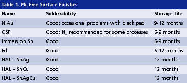
3. Protective coatings of the leads – for the same reasons as with PCBs – have to be specified as Pb-free. Again, a fair choice of finishes meet these demands, but it may be difficult to receive reliable information about them. Many components are not purchased directly from the manufacturer but rather through distributors and agents. These intermediate dealers either lack the information or find it an unnecessary expense to obtain it for customers. Traditionally, purchasing has not specified this parameter and thus the user may face a wall of silence with regard to this crucial piece of information. It is possible to identify the coating in the laboratory. But for the number of different components and the fact that different deliveries may vary in this regard as well, the amount of work required could be enormous and costly. Hence the latter approach would be unrealistic. Whiskers seem to be the spontaneous result of some crystalline growth. Tin and silver are notorious candidates for it. Lead, on the other hand, was used to check and reduce dendritic growth, with considerable success.
Whiskers may lead to intermittent malfunctioning of the product. This sporadic behavior makes them very difficult to trace (Figures 1 and 2). The past few years have seen a fair amount of effort into identifying the phenomenon, particularly by industries for which intermittent failure of product would be especially troublesome (aerospace, automotive, telecom, other security and safety related branches). Investigations3 show that certain countermeasures (nickel coating, reflowing coatings) can minimize the problem. Yet the ideal solution for the post-lead era has not been identified.
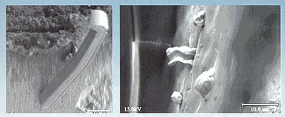 FIGURE 1: Whiskers on a tin surface (a) and on a SnPb surface (b).
 |
 FIGURE 2: Depending on solder volume at the component, longer or shorter whiskers are formed. In the case of SnCu, whiskers can reach lengths of up to 120 µm (60°C/95%RH).
 |
4. Certain features of components play a major role in the long-term reliability of the assembly. The flexibility of the leads is one. For component types such as solder column connectors (SCCs), the increased stiffness of the replacement solders compared to the malleability of SnPb solders will come as an unwelcome property. Other component types are also affected, which has seen a major increase in the use of undercoating. Such measures offer benefits – e.g., increased reliability – and hindrances – e.g., repair after application and cure of undercoats is practically impossible. Much time will be spent compensating for insufficient information on certain component properties.
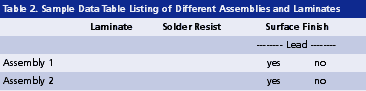
Data collection. Start with a list of all the different assemblies that are manufactured. Add to that the number of boards assembled (per day or month or year). Then, identify the PCBs and their place of origin (by actual manufacturer, if possible).
If possible, add information on aspects such as differences in quality (e.g., number of defects found), type of laminate material, type of solder mask or final surface finish.
Layout and design specifications may provide details on component specification that belong to each assembly. Once their generic identification is in hand, proceed with details such as actual manufacturer(s). This task can take on enormous proportions if the work has to start from ground zero. At the least, for critical components users should have:
- Maximum process temperature allowed.
- Maximum dwell time at highest temperature.
- Largest gradient admissible during temperature rise.
- Largest gradient admissible during cooling.
- Lead finish contains lead (yes/no).
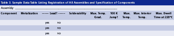
Tables 2 and 3 should serve to develop proprietary aids for data collection.
References
- B. Richards, “Lead-free Soldering – Worlds Apart?” Electronic Packaging & Production, 2002.
- M. Racic and S. Goodell, “No-Lead and Horizontal Hot Air Leveling,” Nepcon West Proceedings, February 1995.
- C. Xu et al., “Whisker Prevention,” IPC Apex Proceedings, January 2003.
Ed.: Future articles in this four-part series will look at wave, reflow and selective soldering equipment, and process changes.
Markus Walter is technical director of SEHO GmbH (seho.de); markus.walter@seho.de.


Press Releases
- RBB Welcomes Shawn Myers as Engineering Project Manager
- ECIA’s Market Sentiment Index Average Hits Five-Year High in June Industry Pulse Survey
- Incap Slovakia invests in cleanroom capability to support semiconductor manufacturing requirements
- Orbit Technologies accelerates growth and doubles production capacity with Europlacer iineo placement machine