Reducing Stencil Wipe Frequency
A new study of nanocoatings allows users to visualize solder paste flow under the stencil.
Do nanocoatings really extend stencil underwipe intervals? As part of a larger stencil study we were performing for SMTAI,1 we decided to include a quick test. We’d take two of our nanocoated fine grain stencils and run one print per wipe vs. 10 prints per wipe on a really complex test vehicle.
The Process of Record (POR) for this PCB is a vac-dry-vac wipe after every print, based on prior experimentation before the nanocoating was introduced to the process. We were almost certain that a tenfold extension of wipe intervals would show a definite decline in print quality, regardless of the coating’s influence.
The results were amazing: not only did not wiping for 10 prints not deteriorate print quality, it actually improved it! The 10 prints with no wipe produced higher yields and better repeatability than the 10 prints with a wipe every cycle. This was no fluke. It happened twice in a row, using two different generations of SAMP nanocoating.
The surprising results ignited a burning curiosity about the performance improvement. The numbers were clear: yields were higher and print volume variation was lower, but we wanted to see what was going on. We devised an experiment to help visualize the interaction between the solder paste flux and the stencil by nanocoating half the stencil’s print area and adding UV tracer dye to the solder paste.
Our suppliers were extremely supportive of our investigation. Indium added UV tracer to Vicor’s usual solder paste so we wouldn’t have to dial in a different material just for the tests. Aculon supplied plenty of NanoClear coating packets and a dyne pen to help develop a robust masking and coating process for our test stencil. Kyzen provided stencil wipes presaturated with a solvent that was tested and approved for both Vicor’s paste and the nanocoating. With all the materials and test vehicles readied, all we needed was some line time to run the tests.
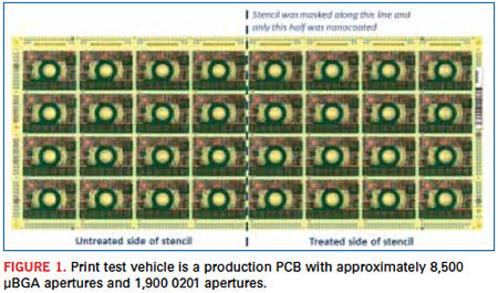
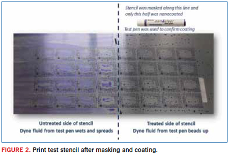
A spare, relatively new, uncoated stencil from a favorite test vehicle – shown in Figure 1 with almost 15,000 apertures crammed into a 3 x 7" print area – was essentially divided into two by temporarily masking half the print area and nanocoating the other half. The PCB is a 4 x 8 array. Using a stencil that was half coated and half uncoated enabled head-to-head comparisons on adjacent 4 x 4 arrays (Figure 2). By holding every other print variable constant, the effect of the nanocoating on stencil cleanliness, print definition and stencil under wipe effectiveness was isolated and obvious. Several tests were executed, and the visible differences were documented with a digital microscope and a UV flashlight.
First, 10 prints with no underwipe. The flux on the bottom of the stencil fluoresced under the UV light to show where it flowed during the printing process. Figures 3 and 4 show the bottom side of the stencil for 0.5mm pitch BGAs, 0.5mm pitch QFNs and 0201s. The top two photos show the underside of the stencil prior to wiping. The apertures on the untreated area demonstrated much more flux wicking and smearing than those in the treated area. In many cases, the edges of the treated apertures are visible, indicating considerably better containment of the paste than the untreated side, where some apertures are already bridged by flux.
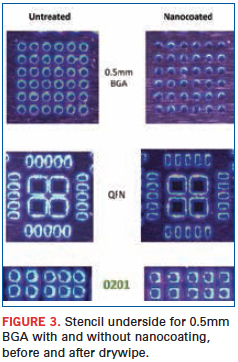
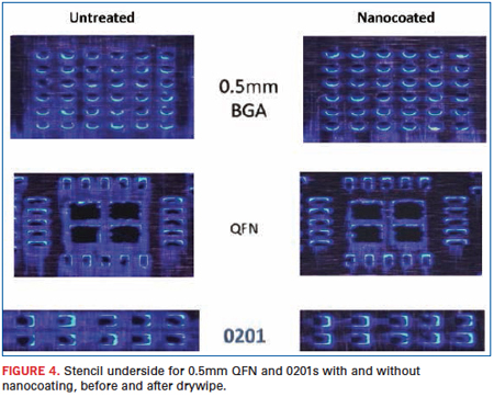
The next test was a vac-dry-vac wipe after the 10 prints, shown in the bottom two photos of Figures 3 and 4. Wow! While underwiping removed the stray solder spheres that impede gasketing from the bottom of the stencil, it did not remove the flux. Instead, it smeared the flux all across the bottom side of the stencil.
Again, the effect of the nanocoating was abundantly clear: the coated area of the stencil responded much better to the dry wipe than the uncoated area, although it still showed some flux residue.
The 10-print test with a vac-dry-vac wipe after every print caused more flux smearing on both areas of the stencil, but the nanocoated side showed less smearing and less paste trapped in the apertures. When a solvent wipe was mimicked by cleaning the bottom of the stencil manually with the presaturated wipes and immediately running the printer’s automatic vac-dry-vac wipe cycle on it, the nanocoated area cleaned up beautifully, while the non-coated side still fluoresced with telltale flux residues. Unfortunately, the microscopy equipment did not capture the images very well; upgraded photographic methods are planned for future tests.
We started the experiment with the hopes of documenting some visible differences in the solder paste-stencil interaction between the nanocoated and non-nanocoated areas. After weeks of planning, enlisting the help of our suppliers and scheduling run time, we were absolutely elated to see such a contrast between the two conditions. But there was something else we were hoping to see in this experiment also – a difference in the paste prints themselves. Starting with our first study on nanocoating two years ago,2 we’ve been noticing that the nanocoated stencils have produced slightly lower transfer efficiency (TE) than uncoated stencils. We have hypothesized that the lower TE is due to crisper print definition, but have yet to formally investigate it.
In addition to photographing the bottom of the stencil, the paste prints were photographed. The objective was to look specifically for differences in print definition, but it was not possible with the BGAs. At a maximum magnification of 40X on the digital microscope, the top-down view was no help, and the scope’s autofocus function did not work well on the angled PCB for oblique angle views. The photos of the QFNs and 0201s, however, undeniably demonstrate the print definition differences.
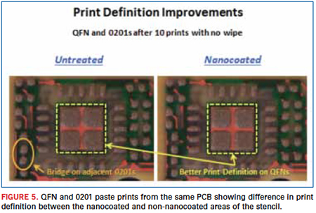
The QFN and 0201 prints shown in Figure 5 were taken from the 10th print with no wipe, and correspond to the apertures shown in Figure 3. The effect of the excess flux/paste smearing on the bottom of the stencil was obvious: a bridge connected two pads from adjacent 0201 components, and the difference in print definition was easily observable in the QFN’s ground pad. It’s only one data point, but a very strong one that supports the hypothesis that the lower TE may be associated with crisper print definition, and necessitates further investigation of the relationship.
All the details of these tests will be published at the IPC Apex conference next month, and as mentioned, the next round of experiments is in the planning phase.
It will take a closer look at the relationship between print definition and TE by taking higher magnification photos of print definition and using the SPI system to capture 3D models as it measures paste volumes. The higher resolution imaging will also be used to depict the effects of different wipe parameters on nanocoated and non-coated areas of the stencils. Two groups of researchers will combine their collective findings on coatings and wipe processes to formulate and execute a comprehensive DoE.
The relationship among stencil coatings, cleanliness, cleanability, print quality and cost savings is currently understood at only a very basic level. There are many
improvements and tradeoffs to characterize, both obvious and subtle, and the mathematics of the relationships will emerge as laboratory research and production implementations continue. This we know for sure: this affordable, accessible coating that wipes on in a matter of minutes makes a big difference in the print process – one we can all see.
Chrys Shea is founder of Shea Engineering (sheaengineering.com); chrys@sheaengineering.com. Ray Whittier is principal SMT process engineer at Vicor (vicr.com).
Press Releases
- Kitron Secures EUR 37M order for Next-Generation Tactical Communication Equipment
- Scanfil Comparison Figures for Updated Customer Groups
- Javad EMS Invests in Inovaxe Smart Storage Carts to Streamline Material Management and Boost Production Efficiency
- ViTrox Announces Strategic Partnership with High Tech Solutions (HTS) to Strengthen Presence in Argentina


