Power Electronics Packages with Embedded Components – Recent Trends and Developments
Results of a cross-industry team’s development and testing of a PCB-based embedded chip technology for an under-the-hood automotive application.
Over the past five years, laminated-based chip embedding has taken a huge step toward industrialization. Meanwhile different products in the low- and medium-power application are commercially available.
One of the first packages was a DC/DC converter called MicroSIP from Texas Instruments, produced by AT&S in high volume.1 Shortly after its release, similar DC/DC converters were found on the market, such as the comparable 650mA DC/DC converter by Rohm Semiconductors, manufactured in TDKs SESUB (Semiconductor Embedded in Substrate) technology (Figure 1). Both were highly miniaturized packages targeting mobile communication applications.
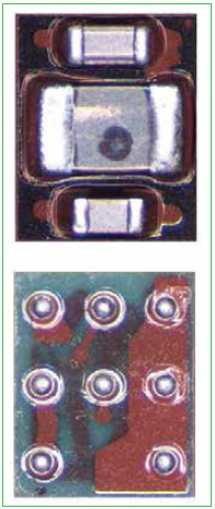
Figure 1. Rohm Semiconductor 650mA DC/DC converter.
In early 2013 Infineon Technologies released its Blade package platform, which is based on embedded chip technology and provides innovative low-voltage MOSFET packages and integrated DC/DC converters (Figure 2) for use in high-end server applications.2
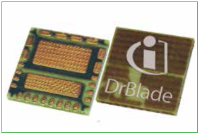
Figure 2. SMD package with two embedded MOSFETs and driver. Source: Infineon
A more complex module was recently found with TDKs smartphone management module. This module contains two embedded die: a power management chip and a 16-bit RISC controller, as well as passive SMDs assembled on top. This module again is manufactured using TDKs SESUB face-up embedding technology (Figure 3).
According to the SYSTEM PLUS teardown report,3 this module provides a 60% size reduction, compared to using conventional discrete devices and BGA packages.
For high-power applications, especially for fast-switching SiC semiconductors, direct connections to the die, avoiding wirebond connections, are a big benefit for the resulting package. Using embedded die and direct copper connections, switching cell inductance can be reduced significantly. The module development described by Hoene, et al4 realizes fast switches with a DC-link inductance of only 0.8nH.
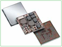
Figure 3. TDK smartphone power management unit.
Automotive control units are increasingly directly attached to their working environment. The advantages are short sensor and actuator paths and fast reaction times. The disadvantage is that harsh environmental factors, e.g., heat, vibration or transmission fluids, are in direct contact with the control units and close to the electronics. In addition, available space under-the-hood for control units is highly restricted. Today’s automotive power devices are based on DCB (direct copper bond) ceramic substrates. Chips, typically IGBTs and freewheeling diodes, are mounted on the DCBs by vacuum soldering. The top sides of the chips are connected by heavy 400µm Al wirebonds. The DCBs are then soldered to CTE-matched AlSiC water coolers, as shown in Figure 5. This technology, however, shows disadvantages, especially a relatively thick construction, reliability limitations due to the Al bonds and high cost for DCB and CTE matched coolers.
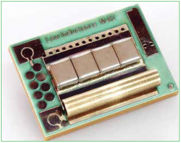
Figure 4. Ultra low inductance module for SiC.
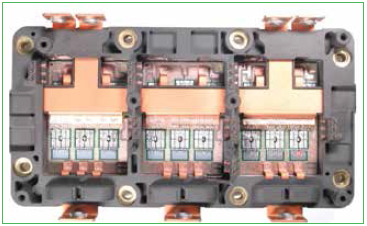
Figure 5. State-of-the-art 80 kW automotive power module with wire-bonded chips on AlN DCB substrate. Source: Continental.
For hybrid engines, additional electronic modules are needed under the hood. In recent models, even in the higher-end versions, available space is highly restricted. Figure 6 shows an example of positions for control units, where they can be attached to a higher-end auto gear box.
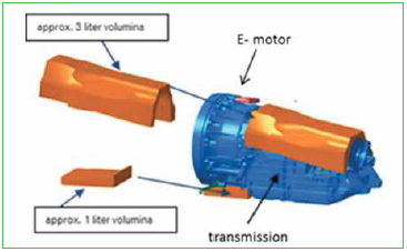
Figure 6. Electronic module attached to gear box.
Keep in mind the overall operating time of control units for electric vehicles will increase. Power electronics have to be designed for 15 years in the field. This means a qualification of 300,000 km or 8,000 hr. To meet future demands for compact, robust and highly functional electronics devices, PCB-based embedded technology offers great opportunities. The embedding process permits different electrical components, conventionally placed on the substrate surface, to be integrated into PCB layers. These special PCBs can be optimized for thermal conductivity. Smaller constructions and lower inductances with higher voltages or higher power densities and improved reliability are expected. It has been demonstrated that embedding very-fast-switching SiC devices into a half-bridge module can result in a stray inductance of 0.8nH.
The HI-LEVEL Project. The HI-LEVEL (Integration of Power Electronics in High Current PCBs for Electric Vehicle Application) project5 teamed representatives from industry (automotive manufacturers and suppliers, semiconductor and material suppliers, PCB manufacturers) and research (circuit design and packaging) to develop the technology, components and materials to realize innovative high-power modules (Figure 7). The goal: to realize highly reliable modules, needed for controlling electrical engines, using PCB-based chip embedding technology. Size and cost reductions are major drivers for the developments. Together they represent a complete value chain for embedded device development and manufacturing. The final goal is the realization of a 50kW inverter for the electric motor of a higher-end hybrid car. In a conventional version, using DCBs and wirebonds, this inverter currently is in manufacturing. The choice of this emulator gives the opportunity to evaluate the embedded version in a proven test environment and to enable a realistic benchmarking.
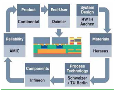
Figure 7. HI-LEVEL Project partners represent the whole supply chain for embedded power modules.
The idea is based on a high-current PCB, on which the IGBT and diodes are assembled using new die attach materials, and then the die are embedded in laminate materials and directly connected using microvia and copper metallization. Additional passive components and the microcontroller can be assembled directly to the high-current PCB. The main topics currently addressed in this project are the highly thermally conductive and electrical die attach, thermal management and the realization of thick-copper substrates.
For die attach, highly conductive, low-temperature and low-pressure sinter materials are being studied. Suitable thermal laminate materials and sufficient heat spreading by the thick copper substrate are required. Therefore, besides all the experimental work, a detailed thermal simulation is performed to determine all aspects that impact the thermal resistance within the module.
The first test vehicle is a 10kW power module. The manufacturing process and the electrical characterization are described here.
Circuit design and test vehicle. The circuit topology realized in the 10kW test vehicle is a simple inverter half bridge consisting of four functional elements, specifically two IGBTs and two freewheeling diodes (Figure 8).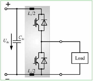
Figure 8. Principle circuit of the 10kW test vehicle.
Each element is implemented using three parallel chips to increase current capacity. The packaging technology permits these elements to be brought close to each other in order to minimize stray inductance of the switching cell. This inductance is responsible for overvoltage during turn-off of each IGBT. A lower stray inductance permits faster switching, which reduces switching losses, or increases the DC link voltage, reducing conduction losses.
Figure 9 shows the PCB layout. The area that represents the switching cell is approximated by a black rectangle. A capacitor bank of eight MLCCs (ceramic capacitors) is used to keep this area small. An added feature in the circuit design is the use of a special type of IGBT chip. These chips are equipped with internal sensors for current and temperature, permitting easy measurement of the junction temperature during operation. Cross-checked by conventional junction temperature measurement methods, the thermal performance of the module can be analyzed. Essential quantities are the thermal resistance Rth and the thermal impedance Zth from die to cooler.
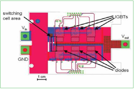
Figure 9. PCB layout of 10kW test vehicle with embedded IGBTs and diodes.
Further, the current in each IGBT chip can be measured separately. Accordingly, it can be tested, if the realized serial connection of the gate contacts is applicable, because it might be that this asymmetrical connection leads to a strongly unbalanced load of the IGBTs during switching.
Figure 10 shows a schematic cross-section of the module. On the base power PCB, six IGBTs and diodes are assembled using low-temperature sintering. The power PCB provides a partial immersion silver metallization for the die attach. The 70µm thick IGBT and diodes are attached to this substrate. The power PCB consist of layers of 100µm thick copper for heatsink assembly, the thermal laminate layer and the 400µm thick copper structures. Embedding of the semiconductors is performed using a standard high Tg prepreg. The embedded die are connected by a matrix of laser-drilled microvias. After desmearing and activation, the microvias will be filled with copper in an electroplating process to provide the best possible electrical and thermal connection. Capacitors will be assembled directly on top of the module, and the control board will be connected to the module by contact banks.

Figure 10. Schematic of 10kW demonstrator module.
Manufacturing process of the 10kW test vehicle. In the first step, the power PCB is manufactured, replacing the DCB used in the conventional module. A stack of a 400µm thick copper sheet, a thermally conductive prepreg and a 100µm copper foil are laminated to produce the base substrate. The thermal prepreg provides a thermal conductivity of 2.5W/mK. Ideally, a 75µm thick prepreg with a thermal conductivity of around 4.8W/mK is required, to replace a 380µm thick Al2O3 DCB, providing the same performance. Therefore, constant review of available materials is in progress. (Materials with a thermal conductivity up to 5W/mK are available, but are in R&D status at suppliers and need further investigation and optimization.)
Structuring of the thick copper layer of the power PCB is performed subtractively through lithography and etching. To prepare the substrate for the silver sinter die attach, an immersion Ag layer is deposited at the locations of the IGBT and diodes only. Following this step, the Ag sinter paste is applied by stencil printing, and the die are placed using a conventional die bonder. Sintering is conducted in a convection oven using a suitable sinter profile with a maximum temperature of 220°C (Figure 11).
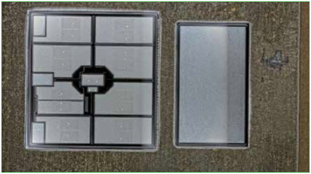
Figure 11. Ag-sintered IGBT (left) and diode (right) to a thick copper substrate.
Figure 12 shows a cross-section of the bond line between a diode with NiAg backside metal and the Cu substrate with Ag finish. The Ag particles in the sinter layer form a continuous net and show a good connection to both interfaces. Nevertheless, this process is still under investigation. Besides the material and process optimization, analytical methods to determine the quality of the Ag sinter layer in the production process are being researched. Methods used for the analysis of chips attached by solder cannot be used here. Acoustic microscopy cannot show delamination between die, die attach or substrate. For process development, cross-sections give valuable analytical results but are not suitable in a volume production environment.
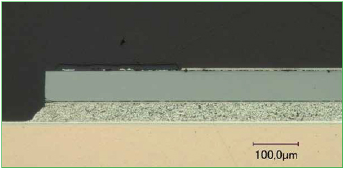
Figure 12. Cross-section of Ag sinter die attach.
Next, the die are embedded. Since a 400µm thick copper layer needs to be compensated for, besides the prepregs for embedding the die, inlays to fill this gap need to be laid up (Figure 13). Lamination is performed using a standard multilayer vacuum press. Press pads are used during this process for uniform layer formation, especially above the embedded die and to guard against chip damage. Even though the build-up is slightly asymmetrical, no significant warpage of the substrate is visible after lamination.
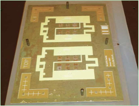
Figure 13. Layup of prepreg an inlay prior to vacuum lamination.
To create the electrical contacts to the embedded IGBT, diodes and the substrate, blind microvia are drilled by laser (die) and mechanical (substrate). The die used in this demonstration provide a NiPd pad metallization, which is generally suitable for laser drilling and copper metallization, but the small process window is small. For volume production, a 5-8µm copper pad metallization would be the ideal choice for the die; this is currently under development. Electrical contact is made by electrolytic copper deposition, filling the via contacts to the embedded die with copper and plating the top copper layer to the required copper thickness of 100µm. Structuring of the top copper layer is again done by lithography and etching (Figure 14).
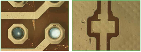
Figure 14. Solder mask prior to etching the top copper layer.
Finally, a final finish is applied to the outer layers, and the module is separated from the larger production panel. Figure 15 shows the final module after separation. The module does not show significant warpage, and the total thickness is around 900µm. The required capacitors and connectors were assembled to the front of the module prior to electrical testing. The backside of the module provides the thermal pads for heatsink assembly.
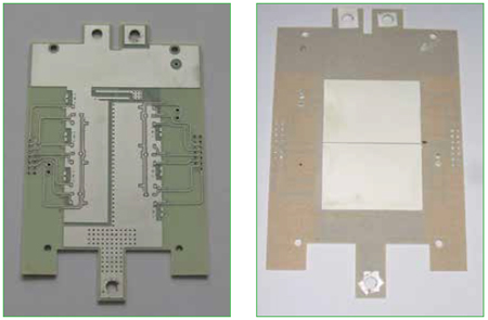
Figure 15. Final 10kW module showing the front (left) and back (right) sides.
Figure 16 shows an x-ray of the final module. The six embedded diodes and IGBT are visible in the center of the module. These modules were electrically tested at the project partner ISEA/RWTH. Figures 17 and 18 show the double pulse test at 1000A and 250V. This test was performed to verify the switching capability of the module. The module shows a switching power of 770A@250V for on, and 970A@250V for off. At 400V input voltage, currents of 500A (on and off) were measured. Note that the significant overvoltage is caused by the test setup, which was using a large current probe, and is not related to the module.
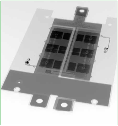
Figure 16. X-ray of the final 10kW module.
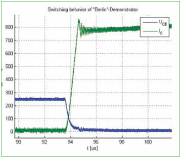
Figure 17. Switching behavior 10kW module “on.” 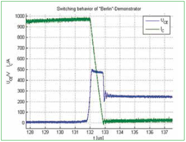
Figure 18. Switching behavior 10kW module “off.”
To demonstrate the capability to transfer the rated power of 10kW, as part of a test setup the module was mounted to an air cooler. It could be demonstrated that the module shows stable behavior at 10kW. Increasing the switching power to 25% overload, stable performance of the module at 12.5kW was demonstrated. The surface temperature over the IGBT reached a saturation value of 85°C after approx. 6 min.
Outlook 50kW module. Realization of the final 50kW module has begun. In principle, the manufacturing of this module is based on its 10kW predecessor. The module, as shown in Figure 19, will be comparable to the conventional module (Figure 5), which permits realistic benchmarking.
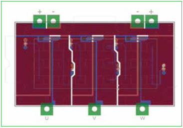
Figure 19. Schematic of the final 50kW module.
Conclusions
Over the last couple of years, the chip embedding technology has gained huge interest for manifold application. Meanwhile, different products in low- and medium-power applications are commercially available.
In a German-funded research project, HI-LEVEL partners from industry and research are developing a next generation of automotive power electronics using PCB embedding technology. A 10kW power module with embedded IGBTs and diodes has been realized. The manufacturing of such modules is based on printed circuit board technologies. The first electrical tests have shown the functionality of the module. Long-term power cycling tests still have to be performed.
The final goal is the manufacturing of a 50kW inverter for an electrical hybrid car. It is expected that embedded technology can fulfill the demanding requirements on
electronics for the future of fully electric vehicles.
Acknowledgments
The authors would like to thank the German Federal Ministry of Education and Research for financial support of the HI-LEVEL project (FKZ 13N11651). They would also like to thank the partners within the HI-LEVEL projects, especially Christoph Neeb from RWTH Aachen and colleagues from Schweizer Electronic, for their support.
References
1. Hannes Stahr and Mark Beesley, “Embedded Components on the Way to Industrialization,” SMTA International, October 2011.
2. Infineon, infineon.com.
3. “Advanced Packaging: TDK-EPC P8009 Module with Maxim Embedded Dies,” www.i-micronews.com/reports/TDK-EPC-P8009-Module-Maxim-Embedded-Dies/8/375/.
4. Eckart Hoene, Andreas Ostmann, Binh The Lai, Christoph Marczok, Andreas Müsing and Johann Walter Kolar, “Ultra-Low-Inductance Power Module for Fast Switching Semiconductors,“ Power Conversion Intelligent Motion (PCIM) Conference, May 2013.
5. For information on HI-LEVEL, refer to www.projekt-HiLevel.de.
Ed.: This article was first published at SMTA International in October 2013 and is reprinted with permission of the author.
Lars Boettcher is Project Manager Embedded Die Tech at the Fraunhofer Institute for Reliability and Microintegration (IZM); lars.boettcher@izm.fraunhofer.de. Stefan Karaszkiewicz is with the Technical University of Berlin. Dionysios Manessis and Andreas Ostmann are with the Fraunhofer Institute.


