Design Practices for Panelization and Depanelization
Assemblers demand a complete CAD data package for more effective manufacturing.
Panelization, also known as the processing of boards in an array format, keeps small boards attached to each other within a single, larger substrate.
Panelization is used to process multiple small boards through assembly, and is becoming more prevalent as board sizes shrink.
There are two primary reasons for using an array scheme: One is to increase throughput, and the other to permit the downstream manufacturing processes to maintain their standard panel sizes. Designing several smaller boards onto a standard 18 x 24" panel permits the fabricator and EMS to use common fixtures for efficient handling, printing, placement and reflow.
On a side note, processing in array format might also help the fabricator in other ways. Smaller boards run the risk of being removed during routing due to the router’s vacuum pressure. Keeping small units in an array can reduce the potential of a small unit being pulled into the vacuum.
Figure 1 shows a 10-up array setup. This particular setup solves several issues. First, it obviates any concern with the size of each individual piece, so the vacuum problem mentioned is moot. Second, the gold fingers are directed outward, for plating purposes, allowing the chamfer to be implemented. Third, multiple boards in a single array panel facilitate assembly by eliminating the need for an additional fixture.
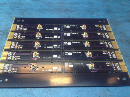
Figure 1. Keeping small units in an array solves several downstream handling and tooling issues.
Depanelization is the removal of the individual PCBs from the panel. This is performed in one of two ways. A saw blade or a manual type tool can be used to remove a board from the panel. In this method, boards are scored, with laminate material removed from the top and bottom of a PCB. Some material is retained in the center to keep the boards in an array format (Figure 2), until assembly and testing are completed.
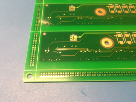
Figure 2. Material is retained in the center to keep boards in an array format until assembly and testing are completed.
Mechanical or laser routing is another process for depanelization. Each has its benefits. Laser routing provides accurate tolerances compared with mechanical routers. The latter can be more cost-effective, but creates considerably more debris during routing. That impacts substrate cleanliness, and the small PCBs could require additional cleaning prior to shipment.
Depanelization is generally performed prior to the final assembly phase or prior to board test. It may be done to meet OEM requirements for the PCBs to be bagged and shipped. Unfortunately, in many cases, OEMs are not completely aware of what is required for depanelization. Generally, they are more accustomed to getting single units delivered, bag to package. On the other hand, PCB assembly requires proper and correct tooling, allowing personnel to process PCBs in panel form to assist with the throughput. Therein lies the disconnect. OEMs may not fully understand how their data are panelized, as long as they get the end-product. Most often they leave panelization up to the assembly personnel. However, CAD data must be made available to properly panelize PCBs.
OEMs often supply incomplete CAD data that omit key ingredients for successful panelization. In most instances, this means only providing data in Gerber format. A complete CAD data package is required, however, showing where actual component boundaries are to be located and the size of those components. Those two key elements are not visible in Gerber.
When the actual body of a component is not seen, the guessing game starts to determine how that component affects the array panel scheme. One solution is to review the bill of materials (BoM) to determine the actual size of a particular package. Another is to review the actual 3D model of the components.
It becomes incumbent on the fabricator to research how much spacing is required between each PCB. Standards can be used to try to answer such questions. However, that approach is a major gamble. A better route is to ask the PCB layout designer to verify whether the spacing between each board could present a problem.
Figure 3 is a great example of how routing was carefully considered prior to fabrication. The part that overhangs the board would potentially interfere with depanelization were it not pre-routed. Also, note the spacing between the board and adjacent part, which permits the board to be spaced properly to accommodate a part near its edge.
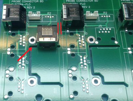
Figure 3. An overhanging part would potentially interfere with depanelization if not pre-routed.
Assemblers face many challenges during depanelization. A component could overhang an edge and fall into the adjacent board. Or it could be in the way of the router or saw blade route during depaneling. Consequently, the EMS would have to change its process to accommodate these shortcomings, or in the worst case, it would not be able to process the array. Such instances mean losing time to depanelize the boards and process them one by one.
Another option for the assembler to combat this particular problem is to depanelize and create a fixture to process multiple boards through the process. But with this comes additional cost and time that was not part of the original scope of work. In cases where individual boards are provided for assembly, a fixture like the one shown in Figure 4 might be necessary.
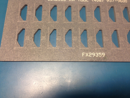
Figure 4. A fixture like the one shown may be necessary in cases where OEMs provide individual boards for assembly.
CAD data not only provides the means for permitting components to be seen, but also when testing issues arise, it provides a road back to the design to search for and locate flaws. Generally, OEMs are not fully aware of the pitfalls of providing incomplete CAD data. The biggest issue is with the netlist.
Take an instance where an open or short is discovered during power ground short testing. However, the assembler has only the netlist. But without complete CAD data, troubleshooting the origins of that particular problem is like operating in the dark. Nets assigned to Gerber data are random and not intelligent. Hence, the
assembler is limited as to the amount and quality of information it can feed back to the OEM.
With CAD data, problems can be isolated and located. For example, a short or connection between two different signals that wasn’t intended can be identified. Those two different nets can be identified, determined where they should go, and what they should be connected to. With only the Gerber data, these faults cannot be identified and corrected.
A complete CAD data package includes the schematic, the CAD layout file it is based on, the Gerber files, and the BoM. However, what occurs with today’s tools is the designer outputs Gerber, the generic format most fabricators use.
Intelligent files, such as ODB++ or IPC-2581, are similar to a CAD platform in their completeness. Users can extract insertion data and get net names, and assemblers can use that data to create pick-and-place files.
OEM Benefits
There are multiple benefits to the OEM for providing a full set of CAD data, including stability, time and thoroughness, to name a few. A universal format that major software companies support avoids potential issues associated with a software tool’s ability to load a given format.
It is time-consuming to load Gerbers, drills, drawings, netlist files, and so on. An intelligent file running various analyses can be virtually instantaneous. Thoroughness comes into play downstream, when one might need to start troubleshooting or isolating a potential open or short, or perhaps even consider how to optimize panelization.
Detailed data streamlines the process and obviates the assembler from revisiting PCB layout for answers to simple questions. In effect, the assembler is permitted to import data much faster and with no errors in translation.
A complete CAD data package permits the assembler to review all the components on a board. It will identify often-overlooked scenarios such as hanging parts overlapping the edges of the board, and parts flush to the edge. In cases like these, panelized PCBs cannot be processed due to those overhanging parts. If they’re not depanelized, assembly problems may subsequently occur. In turn, a new stencil and extra tooling may be required, adding cost and time.
Other Issues
An incomplete CAD data package could lead to material waste. If the overlap for a component is unknown, assembly personnel will guess. PCBs will then be spaced apart accordingly. At the same time, more FR-4 material real estate than necessary may be used, resulting in added cost. What’s not taken into account is the additional material used for tooling. That can increase cost, as more material is used.
“Breakaway holes” or “mouse bites” (Figure 5) are other post-assembly concerns. These are tiny holes drilled into the board, permitting small PCBs to be retained in an array format. The drilling leaves pieces of material that an operator eventually clips with a snip tool to help with throughput. OEM input often lacks such details. In cases like this, it’s learned after the fact that the OEM’s PCBs needed to have smooth edges.
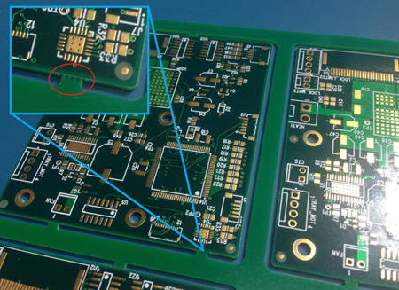
Figure 5. Breakaway holes or mouse bites can help keep small PCBs in array format, but OEM data files are often lacking this information.
When this issue is brought to the assembler’s attention, those mouse bites are manually filed, but the extra work increases labor cost. An alternative approach is a route and V-score type of panel that can be implemented so edges are smooth and jagged holes that need to be filed eliminated.
Other issues can arise if tolerances aren’t specified in the drawing. It’s not normal procedure for a tight tolerance to be specified. Most designers are accustomed to using a standard +/-10% tolerance and failing to account for everything else that will be used. Fixtures, stencils, the bare board itself, and other aspects are associated with panelization. These tolerances are cumulative and could create problems later in the build. It’s highly important to take a close look at tolerances needed coming out of assembly.
Cumulative tolerances take into account the limitations of processes and equipment from all aspects of the build. That includes the limits of the component manufacturer, fabricator, tooling house, assembler and so on. Each plays a part in the result relative to an OEM customer’s requirements. Put another way, ignoring cumulative tolerances has the highest probability of adversely affecting OEM product goals.
Not taking this into account is especially damaging to small and extremely small form-factor PCBs and associated components like µBGAs and µCSPs. Or those problems could affect high-speed PCB performance where the smallest imperfection means the difference between a functioning and nonfunctioning unit.
Also, registration concerns are associated with yield issues when processing PCBs in panelization form. The more boards processed on a single panel, the more the registration tends to be off from center. The manufacturer’s materials can shift for various reasons; machines creating circuit images can change. The more images on a panel, the more registration tolerances can accumulate and cause an image to shift or the material to move.
The solution most often used is to reduce the number of units on a panel to a size that can hold tolerances to acceptable limits. The number may go from 50 to 30 boards on a single panel as a way to increase the yield. This way, assemblers can better control their processes. Newer technologies like laser direct imaging (LDI) and laser drilling can assist in this area, permitting fabricators to hold and maintain considerably tighter tolerances than previously possible.
Phil Lerma is fabrication manager at NexLogic Technologies (nexlogic.com); info@nexlogic.com.


