

Dedicated vs. Flexible Board Support
A good seal between stencil aperture and solder pad ensures the best solder paste deposition.
Enhanced functionality demanded by today’s increasingly miniaturized PCBAs has added to their complexity and density but has also decreased their rigidity. PCBs used to be more rigid and less dense. Solder printing of double-sided boards was performed using standard support pins. In some cases, customized tooling was required to ensure board support.
Today, dedicated tooling and flexible support systems are more frequently employed than ever before. They are easy to set up and provide excellent support. This is in part because the support pins typically supplied with the printer are often perceived as being too difficult to set up, and there never seem to be enough to properly support the board.
Why are organizations moving toward dedicated or flexible supports, instead of the inexpensive support pins that come with the equipment? PCB assemblers have found the process of setting up the support pins depends highly on the user. The manufacturing engineer can document the best methodology for determining the optimum locations for best board support. Implementation will be the responsibility of the operator, however.
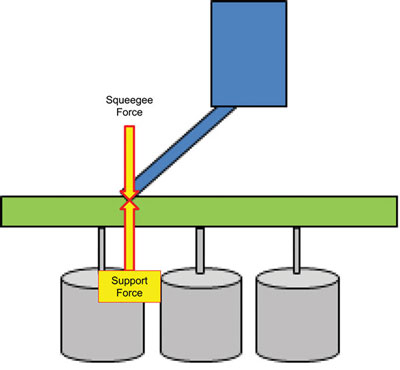
Figure 1. Ideal forces at one point. Note there are only two forces, each cancelling the other.
Manual support pins are efficient and flexible. That flexibility is also its vulnerability, however. A single missing or misplaced support pin can severely impact product quality. A missing pin can change the PCB rigidity, causing more variation in solder paste deposition (FIGURE 2). This variation is sometimes overlooked, especially if it does not result in a visual defect after the print. A misplaced support pin can damage a component on the bottom side of the board and thereby change the board contour (FIGURE 3). The defects caused in both instances may emerge later in the process, i.e., post reflow. This is one reason manufacturers are moving away from support pins and opting for a different solution.
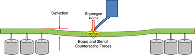
Figure 2. When there is not enough support, the stencil/board counteracts the squeegee force.
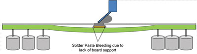
Figure 3. One effect of insufficient PCB support is misregistration between apertures and solder pads. There is a poor seal between them, and solder paste bleeds out from under the stencil aperture.
One solution is a system of dedicated support plates. These are easy to set up and guarantee repeatable results. However, they require time for development (design) and are difficult to modify once delivered. Not every facility has a machine shop available, so the plates must be fabricated externally. Some products cannot be shipped outside the facility due to certain regulations. Therefore, the process engineer must provide the key dimensions required to design and manufacture them without a sample PCB. A lead time is also associated with this process. The logistics and traceability of these plates are also critical. They must be tagged, and all changes documented and implemented across all the plates created for the same product. Every product will require a set, and if there are multiple lines running the same product, a set for each line is required. These plates must be properly stored and maintained, since printing process defects may surface downstream. A quality improvement that requires a modification of a plate will be expensive and take time to implement.
Flexible tooling lies between the two extremes in the middle of the spectrum. As named, it is flexible and easy to set. Flexible tooling works well when properly maintained, and when the minimum number of modules required per product is installed. These systems require integration with the screen printers. This is easy to do and best done before delivery at the screen printer manufacturer’s site. These systems are not especially effective when the PCBs are extremely warped. This is because the systems conform to the board’s contours, and as a result, warpage is difficult to correct once the system is locked (FIGURE 4).
Figure 4. Flexible support system. Note how the system conforms to the PCB bottom’s profile.
Support systems like the one shown in Figure 4 have advantages and disadvantages. Another way to make the support pin approach more attractive is with automation (FIGURE 5). The pins have the rigidity of the dedicated plate, and using automated pin placement, it becomes a flexible support system. With the aid of software, pin locations are assigned, and the screen printer automatically places them in the predetermined location. The system also checks to ascertain that all pins are in their proper locations. Also, pins can be added in the program if more support is required at a specific location (FIGURE 6). Once the program is modified and propagated across the machine, the new support pin array will be executed automatically, without the need for operator intervention.
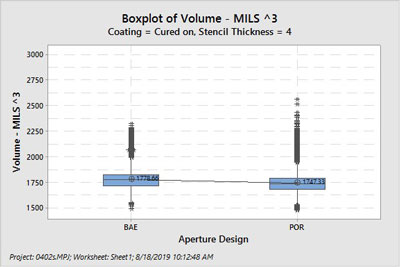
Figure 5. Automatic support system. This system places, removes and verifies pin position.
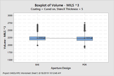
Figure 6. Cause-and-effect (fishbone) diagram of a good print. Board support is a key factor in achieving a good print.
Our hypothesis: There is no significant solder paste deposition variation between a dedicated support and an array of support pins.
Experiment
To test our hypothesis, a double-sided board (FIGURE 7) was printed using a dedicated support plate (FIGURE 8), and then with support pins (FIGURE 9). A customer provided the board, dedicated support plate, stencil, and screen printer program. Thus, we can assume the user fine-tuned and validated the configuration . Two different configurations were evaluated.
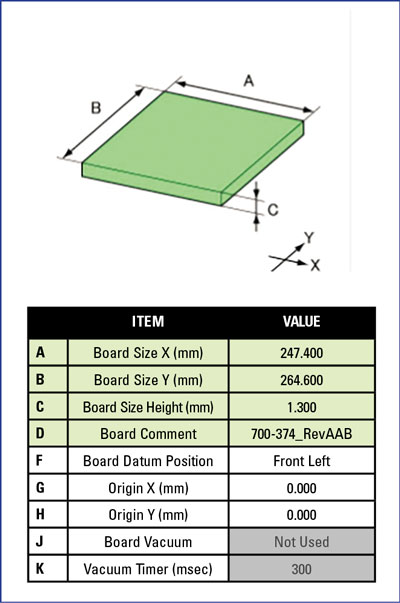
Figure 7. PCBA panel dimensions.
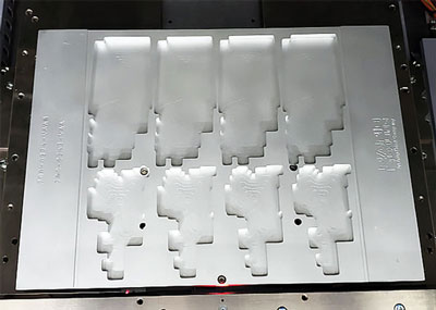
Figure 8. The dedicated support plate.
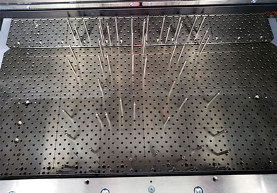
Figure 9. The support pin array.
The first configuration (baseline):
- Customer’s dedicated support plate
- Customer’s screen printer program
- Customer’s 5 mil-stencil, laser cut, and with nanocoating (Nanoslic) (FIGURE 10)
- 10 PCB assemblies with components on the first side
- 4-up panel, with dimensions x = 247.4mm, y = 264.6mm, and t (thickness) = 1.30mm. The smallest passive component was an 0402, and the smallest pitch was 20 mils.
- Koki S3X58-M406-3 Type IV solder paste.
The second configuration:
- Screen printer support pins – 76 support pins were used
- Customer’s screen printer program
- Customer’s 5 mil-stencil, laser cut, with a lubricating nanocoating (NanoSlic)
- 10 PCB assemblies with components on the first side
- 4-up panel, with dimensions x = 247.4mm, y = 264.6mm, and t (thickness) = 1.30mm. The smallest passive component was an 0402, and the smallest pitch was 20 mils.
- To avoid any noise during solder-paste deposition measurement, a new group of the same PCBAs were used to ensure there will be no noise in the measurements due to residues left during PCBA cleaning.
- Koki S3X58-M406-3 Type IV solder paste.
A new jar of solder paste was used to eliminate any interaction between the solder paste and print process that might skew the results.
All printed PCBAs were inspected with a solder paste inspection (SPI) machine. The same SPI program was used for both conditions. Recorded data were analyzed to determine differences in the resulting print between the use of a dedicated support plate versus support pins.
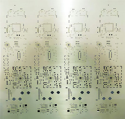
Figure 10. Bottom side of the stencil used for the evaluation.
Results
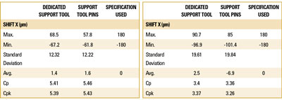
All data were analyzed using Yamaha YSi-SP SPI offline SPC software. The results shown in FIGURES 11 to 14 are derived directly from the SPI application. Upon examination, no meaningful difference between the dedicated support plate and support pin printing results could be discerned.
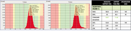
Figure 11. Dedicated support plate vs. pins: volume results.
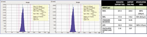
Figure 12. Dedicated support plate vs. pins: height results.
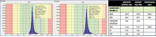
Figure 13. Dedicated support plate vs. pins: area results.
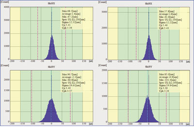
Figure 14. Dedicated support plate vs. pins: offset results.
Conclusion
There is no significant difference between the results obtained with either support media (dedicated) or with pins. Therefore, we see that support pins can provide optimum board support during printing, without compromising the gasket between the PCB and stencil. Based on these results, we are proceeding to run products using only support pins. This will greatly reduce the time, resources and cost required to build a dedicated support plate for each product.
Automated support pin placement ensures the pin array will be the same every time, and the program is loaded without need for operator intervention. It is shown that an array of support pins can provide excellent support. Therefore, the quality of the solder deposition on the PCB will yield good results at the end of the process, every time a product is set up.
The advantage of the dedicated tooling plate is it provides the same support across the PCB every time and is easy to set up. However, it is not easy to modify and creates inventory. A screen printer that automatically sets the support pins will eliminate tooling inventory, provide process flexibility, and preserve yield quality.
Table 1. Dedicated Support Plate vs. Pins Offset Results
, CSMTPE, is product application manager at Yamaha Motor Corp. (yamaha-motor.com); miguel_colomer@yamaha-motor.com.


Press Releases
- Altus Adds LPKF CuttingMaster 3290 to Depaneling Portfolio
- Kurtz Ersa Partners with E-tronix for Sales in Illinois and Wisconsin
- XLR8 EMS Welcomes Raul Jorge Lopez Jr. as Director of Program Management and Procurement
- Koh Young America Promotes Ramiro Mora to Lead Service and Applications in Mexico and South America