

An Automated Tin Whisker Risk Assessment Process Resulting in Significant Cost Savings
How a modified design tool automated and standardized TWRA measurement.
The European RoHS Directive mandated that by July 2006, lead would be removed from electronics assemblies. In response, the electronics industry introduced more lead-free components into the supply chain. US military and medical device companies were exempt from this legislation. This exemption is rapidly changing.
Tin-lead parts obsolescence has become an acquisition issue for the military. The risk is alternative RoHS-compliant parts typically substitute pure tin for traditional tin-lead finishes. Pure tin can grow electrically conductive whiskers that may dislodge or short, causing failure (FIGURE 1). To mitigate the risk, the company developed a tin whisker risk mitigation policy that requires hardware programs to develop and implement a tin whisker mitigation plan.
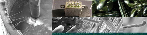
Figure 1. Tin whiskers growing from a transistor assembly (images courtesy of NASA).
Performing tin whisker risk assessments has become a schedule-driving, labor-intensive process. The engineering team’s vision was to develop and implement an automated tin whisker risk assessment (TWRA) process that would reduce manual work and save program cost and schedule.
Engineering worked with the printed wiring board design group to automate the TWRA process using a new approach and evaluated 12 new printed circuit board assemblies using the new process. The average measurement time was reduced approximately 97% per PCB. Furthermore, engineering archived each PCB analysis in a common data management system, allowing easy access for future leveraged designs.
Over a 12-month period, Raytheon business units released a large number of new PCB designs. If this new automated measurement system is employed throughout the company, the potential savings is significant.
Conventional Approach
In the past only a few components were manufactured with only a pure tin finish option and no option for tin-lead plating. Tin-lead component finishes were readily available. Therefore, only a few components required tin whisker risk mitigation. As the RoHS legislation went into effect in July 2006, more component manufacturers transitioned to a RoHS finish (e.g., nickel palladium gold, pure tin, or gold finish), tin being the prevalent option. Companies that had high reliability requirements (aerospace, military, medical) had to spend more time evaluating tin whisker risk in their designs, resulting in increased cost.
Engineering must evaluate each component in the bill of materials for contact finish type. Each component type can be seated in multiple locations on a PCB. If the component is a pure tin finish, a tin whisker risk evaluation is required for every component instance. A key risk factor in the tin whisker risk evaluation is the conductor gap spacing between adjacent components and the component lead spacing itself. The smallest gap spacing measurement identified at each component instance is used as a risk factor dimension in the TWRA to determine the component instance’s risk score. Multiple measurements might be necessary for each component location to determine the smallest gap spacing.
Note the TWRA is not just evaluating component lead spacing. It is also critical to measure the spacing of the adjacent components to determine the complete tin whisker risk. Based on historical data, it can take significant engineering labor resources to complete this task on a densely populated PCB, and to produce new artifacts. This analysis is time-intensive, and it is imperative the data generated from the evaluation be archived in a central repository for access and reuse in future analysis.
TWRA Algorithm
The engineering team proposed an innovative solution of automating the conductor gap spacing measurement process to reduce costs and reduce schedule impact. The TWRA algorithm requires a conductor gap spacing. A key part of this conductor spacing risk factor is the minimum line of sight gap between a tin-coated surface and the nearest conductor (FIGURE 2). Each tin-coated component instance can have multiple components next to it, which must be measured. The smaller the gap, the higher the risk. Manually gathering these measurements is an enormous task to complete on a PCB assembly, where the average number of component instances may be greater than 1,000, each requiring measurement to an adjacent conductor.
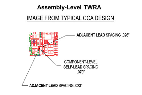
Figure 2. Assembly-level TWRA.
The engineering team already utilized design tools that automate inspection, producibility and tolerance validation for the physical PCB. Engineers use these tools to ensure the assembly of the PCB, and physical layout rules meet specific standards prior to prototype. This process improves assembly yield and reduces labor content. This process capability is critical to assess component gap spacing between a tin-coated surface and any other nearby conductor surface.
The value of these tools’ performance capability and potential cost reduction was recognized, if these tools could be modified to assess component lead spacing to adjacent conductive components, as needed for the TWRA. The team considered use of one of the design tools that could be automated specifically to measure component gap spacing from lead-to-lead of adjacent components (FIGURE 3). Engineering establishes rules in the design tool. Then the tool checks components, pad stack-ups, pin-to-pad, test points and solder point analysis against product requirements. These design rules are configured against product requirements and guidelines established by manufacturing capabilities and component requirements. Engineering previously had not utilized the process/tool to measure adjacent component lead spacing needed in TWRA.
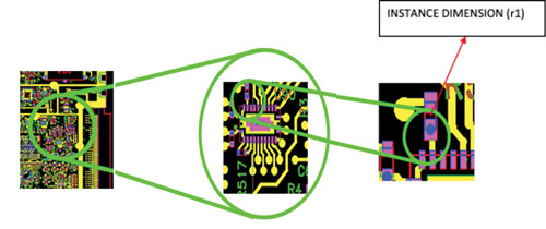
Figure 3. PCB CAD software was modified to measure component gap spacing from lead-to-lead of adjacent components.
Understanding required process requirements, the engineers modified the design tool software and process. Design rules were developed to identify lead spacing on PCBs, from lead to adjacent lead where a TWRA failure will occur under worst-case conditions for Level 2B, in accordance with the Tin Whisker Guidelines and GEIA-STD-0005-2.
Engineering created an output report from the new process (FIGURE 4) that shows any component spacing measurements that failed the design rule. The output report lists:
• ID number
• Component type
• Out-of-specification dimension
• Image of location of a failure
• Reference designators of the two adjacent components.
Engineering can review the data and assess the need for additional TWRA. Engineering can determine if plating materials and self-mitigation considerations are valid and can remove the component risk. Hardware engineering now had a possible solution to automate the TWRA at a reduced labor effort.
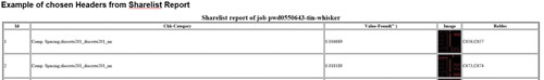
Figure 4. Example of chosen headers from Sharelist report.
Results
Hardware engineering used this tool with the newly configured rules to evaluate nine PCBs for a program. In addition, three other program PCB designs were evaluated using the new TWRA process. A total of 12 PCB assemblies were evaluated using this automated method for TWRA measurement. Based on a historical average, a large fraction of the component instances on the assembly is tin-coated and requires analysis. Some components are known to be dimensionally self-mitigating; i.e., based on dimensions and locations of leads and pad terminations, they are found to be sufficiently small enough to become completely coated with lead-bearing solder during standard PCB reflow soldering.
The tool automated the measurement process between each tin-finished component instance and its adjacent components. This new process is a major time-saver for the component measurement part of the TWRA at the assembly level.
Engineering’s estimate of time and schedule to perform TWRAs using the manual process was unacceptable to meet program cost and schedule goals. Therefore, the new automated measurement process was implemented. Using the reconfigured engineering design tool, spacing data for the 12 assemblies were assessed with significant rapidity. The average time reduction per PCB assembly for the measurement task was reduced 97%. The measurement process eliminated full analysis on most of the components, resulting in only a few components requiring a full factor analysis in the TWRA algorithm. This process change significantly benefited the time for this measurement effort.
An additional benefit is the TWRA output for the entire PCB assembly can be archived by part number as a general document in the data management repository. This repository meets company and customer record management standards. A centralized repository permits easy retrieval for assessment data and work product traceability that support best practices and future rework abilities.
Engineering estimated a significant labor savings of an average 97% measurement time reduction per PCB across businesses, and schedule impact is far reduced. Because the analysis can be performed real-time during the design phase of the board, multiple TWRA preliminary runs can be made in time to give useful feedback to optimize PCB layout, without affecting program cost and schedule.
Tool Implementation
Internal company training on this TWRA tool was held across the businesses in July 2019. This training was held in collaboration with the Lead-Free Tin Whisker Technical Interest Group. Individuals who attended the training became the trainers at each of the businesses. Hardware engineering created a TWRA Automated Measurement Job Aid that was used for TWRA enterprise training. The vision is to supplement training with an easily accessible job aid that documents the process for use across all internal businesses. The TWRA Job Aid has been loaded and approved in the data management system for the whole business to utilize to support their TWRA.
The job aid explains to the user how to generate a TWRA report that identifies components requiring additional analysis after failing the rule for TWRA Level 2B or the rule for TWRA Level 2C, in accordance with GEIA-STD-0005-2. The report highlights the failed component’s location and reference designator. Any self-mitigating components in the report are noted per Tin Whisker Mitigation Guidelines.
Once TWRA is completed, the tool generates a report listing all potential failure sites. The report allows an analyst to focus on components that require additional evaluation and provides critical information such as their locations. Engineering can ignore small components that satisfy the self-mitigation run rules, leaving only a few components to manually evaluate.
All artifacts from the resulting TWRA are collected in a zipped folder. These artifacts include:
• A list of all components on the assembly with information from parts list and vendor part number
• A copy of each required tin whisker algorithm
• A copy of each required gold/palladium embrittlement algorithm
• The TWRA output report
• A summary page, including recommended corrective actions.
Once all artifacts are collected, a general document will be created in the data management tool, and the zipped folder will be attached. The method for archiving the TWRA report includes adopting a naming convention to facilitate retrieval of existing reports. Instead of searching and recording the generated formal document number, a search can be done using the relevant assembly number for easy retrieval.
Next Steps
After training on use of the new tool, scheduling more frequent preliminary TWRA assessments upfront during the design would mitigate the need for redesign after PCBs are manufactured. Engineering could identify these risks early on and modify the design to mitigate any manufacturing issues. This upfront analysis will increase profit by eliminating excess engineering rework, minimize costs of any mistakes and improve reliability. Programs will need this process automation even more when the industry loses its tin-lead exemption.
The next phase of this project will be to merge the output from these assessments with a component database where company part data currently reside. The tool also contains information related to key factors needed for the TWRA. Merging these data will build a system that all engineers can use and share information across all the businesses. Engineering in collaboration with other businesses is looking to assess the work involved in joining the two processes. This merger will reduce time seeking information for the other risk mitigation factors that are specific to the component and can be reused in other designs.
Conclusions
An automated TWRA measurement process was developed using an engineering design tool. This tool use resulted in a 97% measurement time reduction per PCB and a potential significant cost savings across the enterprise in a one-year period.
Using the tool in this manner was an innovative solution that can permit TWRA during PCB layout and manufacturing prebuild review. Using Six Sigma practices, engineering can estimate annualized cost avoidance and assign to prioritize design change decisions. This will address tin whisker risk concerns early in the design process and address any potential reliability issues.
This new process not only saves cost and schedule but provides a document that is ready to archive in an approved repository that is easily accessible for future revision changes.
Acknowledgments
The authors acknowledge the following Raytheon collaborators and analysts: Judiann Sorrells, John F. Shea, Ellen Ferraro, Patrick Lott, Jeffrey Ogorzalek, David Pinsky, Anthony Rafanelli, Ron Mathis, Cheryl Drake, Diane Juhas, Claudia Ludwig, Dan Bradstreet, Delisha Stanley and Eric Lusby.
References
1. D. Pinsky, “Tin Whisker Application Specific Risk Assessment Algorithm,” Proceedings of the 2003 Military & Aerospace/Avionics COTS Conference, August 2003.
2. D. Pinsky and E. Lambert, “Tin Whisker Risk Mitigation for High-Reliability Systems Integrators and Designers,” Proceedings of the IPC/JEDEC 5th International Conference on Lead Free Electronic Components and Assemblies, March 2004.
3. D. Pinsky, “Enhancements to Current Tin Whisker Risk Assessment Methods,” Proceedings of the IPC/JEDEC 11th International Conference on Lead Free Electronic Components and Assemblies, December 2005.
4. D. Pinsky, “An Updated Application-Specific Tin Whisker Risk Assessment Algorithm, and Its Use within a Process Compliant to GEIA-STD-0005-2,” raytheon.com.
5. Tin whisker photo examples, digital photos, courtesy of NASA.
is a principal mechanical engineer and Lead-Free Tin Whisker TIG Co-Chair at Raytheon (raytheon.com); karen_ebner@raytheon.com. is a principal mechanical engineer in the Hardware Engineering Center, Space and Airborne Systems at Raytheon. is an electrical engineer at Raytheon. is a mechanical engineer at Raytheon. is a senior mechanical engineer at Raytheon in the Interconnect and Parts Engineering Group.


Press Releases
- Altus Group Invests in Major Headquarters Expansion to Showcase Complete Turnkey Manufacturing Capability
- ViTrox Americas Welcomes Eric Cruz as Technical Support Engineer
- ECD Strengthens Engineering Team with New Software Development Hire
- ViTrox Americas Welcomes Doug Ennis as Senior Field Applications & Service Engineer