

Sn-Bi Low-Temperature Homogeneous Solder Joint Microstructure, Reliability and Failure Mechanism
How do LTS solders perform under thermal cycling and drop-shock testing?
Several environmental, technology and reliability factors have recently combined to renew interest in the use of tin-bismuth-based solder alloys for motherboard manufacturing. Corporate and government initiatives to reduce greenhouse gas emissions benefit from reduced electricity usage afforded by use of low-temperature solders. Thin electronic components and motherboards experience less warpage at the lower peak reflow temperatures, enabling pitch and form factor scaling, driving technology innovation. A new generation of tin-bismuth solder alloys engineered for increased ductility is enabling SAC BGA-LTS SMT solder joints to meet board-level reliability requirements.
Tin-bismuth (SnBi)-based low-temperature solders (LTS) can be used to create solder joints both when used in conjunction with an electronic package using tin-silver-copper (SAC) solder spheres or a SnBi-based solder sphere. In the case of a SAC-LTS solder joint, the resulting structure is referred to as “hybrid.” For an LTS-LTS solder joint, the structure is referred to as homogenous. FIGURE 1 illustrates the structure of each case.
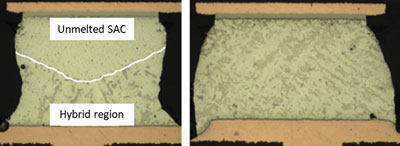
Figure 1. Cross-sectional image of a SAC-LTS hybrid joint (left) and a homogenous LTS joint (right).
When working with hybrid solder joints, it is necessary to consider the ratio of theoretical solder paste volume being printed to the volume of the unmounted BGA sphere used on the component. This is referred to as the paste:ball volume ratio. TABLE 1 illustrates the calculation of the paste:ball volume ratio.
Table 1. Solder Paste Volume to BGA Ball Volume Ratio Calculation
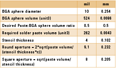
FIGURE 2 illustrates the change in solder joint fatigue performance as the paste:ball volume ratio is modulated. FIGURE 3 shows the typical crack locations and crack types (T1 ti T4). A ratio of 0.5 has been repeatedly demonstrated to optimize the solder joint reliability performance.1 If the ratio is significantly below 0.5, solder joint quality may degrade, leading to all PCB side cracks (T3). A ratio significantly greater than 0.5 may result in small concentrations of bismuth reaching the ball-to-package interface. In the SnBi system, Bi weight percent of 5 to 12% results in significant reductions of elongation2, and this behavior is believed to result in low-cycle, brittle package side failures (T2 cracks) for components built with the excessive paste:ball volume ratio.
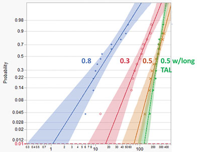
Figure 2. Thermal cycle reliability Weibull for different solder paste to BGA ball volume ratios (0.3 to 0.8).1
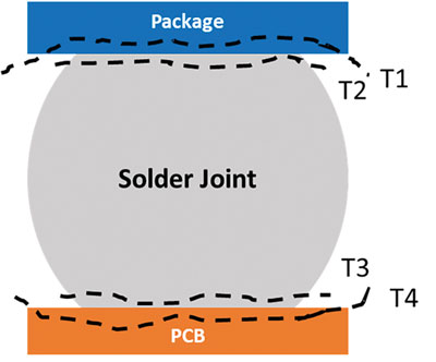
Figure 3. Crack types at different interfaces for a solder joint (T1 – T4) annotated.
For a homogenous solder joint, the Bi is uniformly distributed throughout the joint and the need to control paste:ball volume ratio when designing the SMT process eliminated. By considering the Bi content of the solder sphere and the solder paste, final metallurgy can be achieved that optimizes the elongation performance (FIGURE 4). The paste:ball volume ratio provides an additional process window to modify solder volumes to address warpage or other component requirements necessary to achieve maximum process yields.
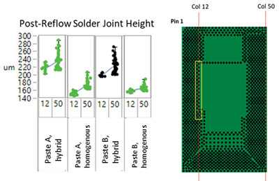
Figure 4. Post-reflow solder joint height difference: hybrid vs. homogenous joints.
Previous investigations have shown hybrid SAC-LTS solder joints formed with eutectic SnBi solders can show reduced mechanical drop capability compared with homogenous SAC solder joints.3 Sn-Bi solders modified with additional doping elements that increase the material ductility demonstrate improved mechanical characteristics.4 It is postulated some portion of the reduced performance of the hybrid SAC-LTS solder joint results from poor control of Bi mixing in the solder joint and small concentrations of Bi at the package side interface, significantly reducing elongation of the solder joint. Tighter control of Bi mixing during solder joint formation or a homogenous LTS solder joint optimized for elongation is expected to show improved mechanical drop capability.
A homogenous LTS solder joint can effectively eliminate a solder joint quality defect referred to as “hot tearing.” In a non-eutectic solder system, during cooling the solder will solidify over a range of temperatures. As the package returns to the room temperature shape, the dynamic warpage creates stress on the solder joints. If the solder joints are not fully solidified during this period, the joint can tear, which creates a crack-like signature post-SMT and may pose a risk to solder joint reliability. For a hybrid joint, this risk is increased by the lack of solder joint collapse during reflow. As the SAC solder ball does not fully melt, the unmelted portion of the joint acts as a standoff and prevents full collapse. Figure 4 shows the difference in post-reflow standoff height of a hybrid solder joint compared with a homogenous solder joint.
Details about hot tearing defects and process knobs to mitigate those in hybrid joints are discussed in a companion proceeding.5 The homogenous solder joint melts completely and creates a full collapse, which has been shown to help eliminate the occurrence of hot tearing (FIGURE 5) and provides a much wider process window.
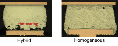
Figure 5. Hot tear defect in a hybrid joint (left) vs. complete collapse under the same SMT process conditions eliminates hot tearing for a homogeneous LTS joint (right).
Given the advantages of homogeneous LTS joints for SMT processing, we examine differences in solder joint morphology between hybrid SAC-LTS solder joints and full LTS solder joints. Post-reflow compositions for different combinations of ball-and-paste metallurgy will be detailed. Finally, component-level reliability performance and failure mechanisms will be compared between SAC-LTS hybrid and full LTS second-level interconnects using different package form-factors.
Experimental Methods
Materials. Two different solder paste materials (referred to as paste A and paste B here) were used for the study. These materials used different flux formulations, as well as different SnBi-based LTS alloys. The Bi compositions of the alloys in paste A and paste B are 50% and 58% by weight, respectively, along with supplier proprietary dopant elements to enhance reliability of the materials. Melting behavior of the alloys was studied through differential scanning calorimetry (DSC) using TA modulated DSC model Q1000. DSC testing used ~10g of paste, which was heated from 25° to 240°C at a ramp rate of 10°C/min. Melting onset, peak and end-of-melting temperatures were recorded.
Thermal cycle reliability: BGA assembly and testing details. To evaluate the thermal cycle fatigue performance of a hybrid joint vs. a homogenous joint, a 16.5mm x 28mm, 0.43mm pitch ball grid array (BGA) component was chosen as the test vehicle. The package used an electroless nickel-electroless palladium-immersion gold (ENEPIG) surface finish and a 250µm solder sphere. Half of the packages were built with a SAC 405 solder sphere, and the other half were built with a SnBi solder sphere with 40% Bi and supplier proprietary dopants. The packages were assembled on a 700µm thick, 15cm x 15cm printed circuit board with copper organic solderability preservative (Cu OSP) surface finish. Each test board had a single package placed at the center of the board. The test board was designed with a daisy chain to allow in-situ continuity monitoring during temperature cycle (TC) testing.
Boards were assembled using two different Sn-Bi LTS solder pastes. To accelerate fatigue failures and reduce testing time, a stencil was designed that did not print paste in certain known high-stress locations (FIGURE 6). Due to the depopulated stencil apertures, no solder joints were formed at those locations. The stress on the remaining joints were increased, thus reducing mean time to failure. A 100µm-thick nano-coated stencil was used with a 237.5µm round aperture for each pad. This resulted in a theoretical solder volume of 0.0046mm3. Compared to the 0.0086mm3 volume of the 254µm solder sphere, the resulting paste:ball volume ratio for the hybrid joints was 0.535, very close to the target 0.5 ratio (Table 1).
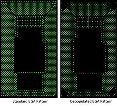
Figure 6. Rows two and three on both right and left long sides of the die shadow region were depopulated in stencil design for thermal cycle testing.
After paste print on a DEK Galaxy printer, 100% paste volume data were collected using a Koh Young solder paste inspection machine. BGA components with both hybrid and homogeneous LTS joints were assembled using peak reflow temperature of 190°C for paste A. Assembly for paste B involved hybrid joint BGA reflow at 175°C peak and homogeneous LTS BGA reflow at both 175°C and 190°C peak. For both pastes, a soak of 60-90 sec. between 100º to 120ºC and a total time above liquidus (set as 151ºC) of 100 to 120 sec. was used. The same reflow conditions were used for hybrid and homogenous joints. All samples were reflowed in ambient air. Post reflow, each board was tested for electrical continuity using a flying probe and then inspected in a Vitrox automated x-ray tool to ensure no solder bridging was present. A corner adhesive was used to provide extra mechanical support at the corners of the package. Prior to initiating thermal cycle testing, one package from each leg was cross-sectioned (XS) to verify solder joint quality.
Test boards were thermal-cycled in an unloaded configuration using a -40º to 85ºC, 30 min. cycle. Electrical continuity was measured continuously in-situ. The sample size was nine boards per leg. Testing was continued until at least 80% of the boards had recorded a failure to permit a Weibull plot to be completed. Eight of nine packages were dyed and pulled post thermal cycling to identify crack type based on the failure interface as shown in Figure 3. The number of cracks larger than 80% of the solder joint area was measured for each crack type. One package from each leg was cross-sectioned to study the microstructure post thermal cycling.
Drop shock reliability: BGA assembly and testing details. A study was completed comparing the mechanical shock capability of a homogenous SAC interconnect, a hybrid SAC-LTS interconnect formed using paste volumes to result in optimum and extended Bi mixing, and a homogenous LTS interconnect. The daisy chain test vehicle was a 16.5mm x 28mm, 0.43mm pitch BGA. The package used an ENEPIG surface finish and a 250µm solder sphere. Half of the packages were built with a SAC 405 solder sphere, and the other half were built with a Sn-Bi solder sphere with 40% Bi and supplier proprietary dopants. For the hybrid and homogenous LTS solder joints, paste A was utilized. The homogenous SAC solder joints were formed using a SAC 305 solder paste. The BGA packages were soldered to a 700µm-thick, 30.5cm x 30.5cm test board. No corner adhesive was used. For this testing, the BGA joints were fully populated, as no-time-to-fail acceleration was required. The test board was designed with a daisy chain to permit solder joint electrical continuity to be continuously monitored in-situ during drop testing.
Mechanical drop testing was completed using a drop table and a variable acceleration (G) level, 2 ms pulse, ½ sine. The sample size was 10 boards per leg. For each sample, five drops were completed at a starting G level of 80G. If no electrical fails were recorded, the G level would be increased by 5G and five drops repeated. Testing continued until all samples had recorded an electrical fail. Capability is reported as <1% fail at 90% lower confidence limit (LCL).
Results and Discussion
DSC Results. Both LTS paste materials showed comparable melting behavior (TABLE 2) despite different Bi composition.
Table 2. Melting Behavior Comparison for Paste A, Paste B, and LTS BGA Spheres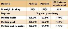
Post-SMT/pre-reliability characterization. One board from each SMT leg was cross-sectioned post-SMT (Figure 4) along column 12 of the package. This column typically exhibited the highest stress solder joints in historical thermal cycle testing on the package. Representative scanning electron microscope (SEM) images are shown in FIGURE 7. Overall, hybrid joint microstructures were comparable for both paste A and paste B.
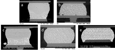
Figure 7. Post-SMT microstructure for (a) paste A hybrid 190°C peak, (b) paste A homogeneous 190°C peak, (c) paste B hybrid 175°C peak, (d) paste B homogeneous 175°C peak, (e) paste B homogeneous 190°C peak.
Temperature cycle testing results. All thermal cycle testing failures occurred in the die shadow region around the central cavity of the package. Thermal cycle Weibull plots (FIGURES 8 and 9) showed a significant improvement in the failure predictability (β parameter) for homogeneous LTS joints over SAC-LTS hybrid joints. The characteristic life (α), however, was lower for homogeneous LTS joint with paste A, whereas it was higher for homogeneous LTS joint with paste B for both 175°C and 190°C peak reflow temperature (TABLE 3). These trends for paste A and paste B are consistent with earlier lab level mechanical testing, where paste B showed better performance than paste A in mixed mode fatigue testing.6
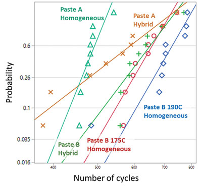
Figure 8. Thermal cycle failure Weibull plot for hybrid vs homogeneous LTS joints.
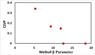
Figure 9. Crack location variability parameter (CLVP) vs. Weibull β parameter.
Table 3. Thermal Cycle Reliability Results with Crack Type Statistics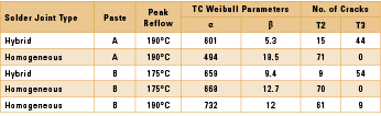
Homogeneous joints also help reduce the microstructure variation typically observed in the hybrid joints. For the hybrid joints, the natural variation in the extent of Bi exposure at the package side as cycling progresses is hypothesized to account for the larger variation in cycles to fail. Previous research4 shows SnBi solder joint performance reveals less capability when paired with NiAu-based surface finishes. For the test vehicle in this study, a homogenous LTS solder joint is expected to fail preferentially at the ENEPIG interface (package side). Literature4 also shows historically that a homogenous SAC solder joint should be more capable than a hybrid SAC-LTS joint, unless the homogenous SAC + ENEPIG has low concentrations of Bi. For the test vehicle in this study, assuming no Bi exposure at the package side, failure location is expected to be at the PCB side.
For both pastes, the majority of failures for the homogenous solder joints was at the package (ENEPIG) interface, which is consistent with the expectation. Only paste B reflowed at 190°C, with LTS BGA showing a few failures at the PCB interface, as shown in Table 3. These cracks are fatigue-driven in the bulk solder (FIGURE 10). In the case of the hybrid solder joints, most of the failures were located at the PCB (OSP) interface, consistent with expectations. A smaller number of failures were noted at the package (ENEPIG) interface, however. As evident from the crack location variation, an inconsistent failure location results in a lower β parameter. To help with the argument, we define a crack location variability parameter (CLVP) as:
CLVP = minimum (No. of T2 cracks/No. of T3 cracks, No. of T3 cracks/No. of T2 cracks)
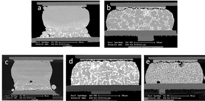
Figure 10. Post-TC microstructure for (a) paste A hybrid 190°C peak, (b) paste A homogeneous 190°C peak, (c) paste B hybrid 175°C peak, (d) paste B homogeneous 175°C peak, (e) paste B homogeneous 190°C peak.
For hybrid joints in this study, no. of T3 cracks > no. of T2 cracks. Hence CLVP is T2/T3, whereas, for homogeneous LTS joints with predominant T2 failures, CLVP is T3/T2. This parameter captures the consistency of cracking locations for solder joints. As observed in Figure 9, it has an excellent correlation with Weibull β parameter. This further asserts variable cracking in a solder joint can impact thermal cycle life predictability.
A microstructure study using SEM showed the best performing homogeneous LTS leg, paste B with 190°C reflow, had more refined Bi-phase post thermal cycling compared to the rest of the two homogeneous LTS legs. The higher Bi-phase refinement can help pin a crack at the Bi/Sn interface, whereas larger Bi particles will lead to a crack along the Sn/Bi interface or through the bulk of the brittle Bi-phase.
Drop-shock testing results. All failures in the drop-shock reliability testing were at the package corner, unlike the thermal cycle testing. Failed samples from the drop-shock testing were submitted to a dye-and-pull process, and then crack type was documented. For the homogenous SAC samples, the primary failure location was cracking under the PCB pad into the board laminate (pad crater). Both hybrid sample legs cracked preferentially at the solder joint-PCB pad interface, indicating the hybrid SAC-LTS metallurgy is weaker than the ENEPIG-SAC interface. In the homogenous LTS samples, cracking occurred preferentially (>70% cracks) at the package side interface (T2 crack). SEM microstructure study confirmed the findings (FIGURE 11).

Figure 11. Homogeneous LTS (left) vs. SAC-LTS hybrid (right) joints showing failure post-shock test.
TABLE 4 summarizes the mechanical drop capability for each experimental leg. The homogenous SAC samples recorded the highest capability value. As was expected, the hybrid SAC-LTS samples built to create excessive Bi mixing showed reduced performance compared to the hybrid samples built to optimize Bi mixing. The homogenous LTS samples showed greater capability than the hybrid samples and performed almost as well as the homogenous SAC units for the critical-to-function (CTF) pin locations.
Table 4. Mechanical Drop Capability Results Versus Solder Joint Construction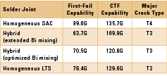
Conclusions
Homogeneous LTS joints are expected to reduce SMT process complications, leading to higher predictability in the solder joint microstructure, reliability performance, and elimination of hot tearing defects. The current study shows that with the right material choices and correct process parameters, homogeneous LTS joints perform significantly better than hybrid joints in both thermal cycle and drop-shock reliability. In addition, a correlation needs to be established between a solder joint life in actual use conditions and thermal cycle life, as a Bi diffusion-driven mechanism may play a role in failure, along with conventional intermetallic compound growth-driven failure in SAC solder joints. This study is applicable for both SAC-LTS hybrid and homogeneous LTS BGA solder joints, which are expected to be highly relevant with increased adoption of SMT LTS technology in the industry.
Acknowledgements
Nilesh Badwe would like to acknowledge Yi He for DSC measurements. Nilesh Badwe and Ou Jin appreciate help from Jeff Cook with thermal cycle data plotting. All authors thank Mukul Renavikar, Srinivasa Aravamudhan, Raiyo Aspandiar, Eric Brigham, Satish Parupalli and Steve Folsom for key input and suggestions during the entire evaluations.
Reference
1. Shubhada Sahasrabudhe, Scott Mokler, Mukul Renavikar, Sandeep Sane, Kevin Byrd, Eric Brigham, Owen Jin, Pubudu Goonetilleke, Nilesh Badwe and Satish Parupalli, “Low Temperature Solder – A Breakthrough Technology for Surface Mounted Devices,” IEEE 68th Electronic Components and Technology Conference (ECTC), May 2018.
2. Hisaaki Takao, Akira Yamada and Hideo Hasegawa, “Mechanical Properties and Solder Joint Reliability of Low-Melting Sn-Bi-Cu Lead-Free Solder Alloy,” R&D Review of Toyota CRDL 39, no. 2, 2004.
3. Scott Mokler, Raiyo Aspandiar, Kevin Byrd, Olivia Chen, Satyajit Walwadkar, Kok Kwan Tang, Mukul Renavikar and Sandeep Sane, “The Application of Bi-based Solders for Low Temperature Reflow to Reduce Cost while Improving SMT Yields in Client Computing Systems,” SMTA International, September 2016.
4. Seiki Sakuyama, Toshiya Akamatsu, Keisuke Uenishi and Takehiko Sato, “Effects of a Third Element on Microstructure and Mechanical Properties of Eutectic Sn–Bi Solder,” Transactions of the Japan Institute of Electronics Packaging, vol. 2, no. 1, 2009.
5. Todd Harris, Kevin Byrd and Nilesh Badwe, “Root Cause and Solution to Mitigate the Hot Tear Defect Mode in Hybrid SAC-Low Temperature Solder Joints,” SMTA International, September 2019.
6. Satyajit Walwadkar, Suresh Guthikonda, Raiyo Aspandiar and George Hsieh, “A Novel Approach to Determine Mechanical Fatigue Performance of Solder Material using Single Solder Joint Test,” SMTA International, October 2018.
Ed.: This article was first published in the SMTA International Proceedings and is reprinted here with permission of the authors.
, , , are with Intel (intel.com); nilesh.u.badwe@intel.com.


