Nepcon Japan Highlights AI, 5G, and Packaging and Assembly Trends
ADAS auto electronics require zero-defect components.
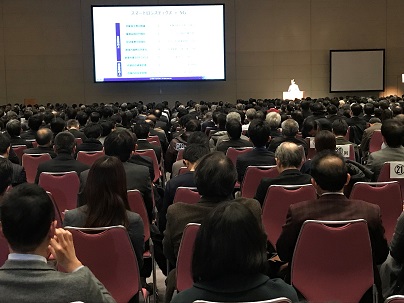
With construction of a new venue for the 2020 Olympics in Tokyo, the annual Nepcon Japan show was split into two parts this year. There were 67,169 visitors to see more than 2,100 exhibitors. A reported 24,323 people attended the conference presentations. Exhibits included automotive and electronics. The electronics R&D and manufacturing exhibits included IC and sensor packaging, LED and laser diode technology, PCB, SMT, test and measurement, components, devices, and materials. Many highly attended conference sessions focused on 5G, AI, and automotive electronics (FIGURE 1).
Automotive electronics. Automotive electronics, autonomous driving and electric vehicles (EVs) were the main focuses of the presentations in Automotive World. Nissan described the evolution of advanced automotive technology and described how the need to reduce CO2 emissions is driving the movement toward electrification. Evolving technologies such as the electric vehicle battery, including cell-energy density and volume, have improved cruising range and charging.
Urbanization and optimum mobility coupled with geriatric drivers create the need for autonomous vehicles. Speakers described breakthroughs in advanced driver assistance systems and autonomous driving (ADAS/AD), especially 360° viewing. Toyota presented its approach to autonomous driving, and Nvidia promoted its GPUs. Xilinx indicated 170 million of its devices have been shipped for automotive use. The Xilinx FPGA technology as an AI solution was presented, and challenges in object recognition were discussed. A design concept for automated parking assist using deep learning was presented. Nissan described its driver assistance technology. Volkswagen presented its adaptive Autosar. Robert Bosch talked about its safe power net solution for autonomous driving, and Continental described its views on AD. Honda and others introduced the concept of Mobility as a Service (MaaS), where connected autonomous electric cars can be shared. Technologies such as 5G and Cellular V2X were discussed by the 5G Automotive Association and Continental. Hitachi talked about design for safety with high-reliability systems. Autosar discussed the safety and security of autonomous driving, highlighting its software framework for autonomous vehicles. Infineon described trends in component packaging, including radar modules packaged in fan-out wafer-level packages and lidar systems using MEMS mirrors. Velodyne Lidar proposed standardization of range detection and targets, as well as lidar mounting and analysis methodology. After listening to many presentations, the drive for automotive electronic components with zero defects is clearer. No room for error in this application!

FIGURE 1. Full house for talks at Nepcon Japan.
Advanced packaging. High-performance packaging trends, including chiplet developments, were presented by several consulting firms. Chiplet solutions from AMD, Intel and TSMC were mentioned. The high-performance packaging discussion was not limited to chiplets. Fujitsu’s booth featured its server processors packaged in flip-chip ball grid array packages. Fujitsu’s supercomputer application features its logic device plus Samsung’s HBM, assembled on a silicon interposer using TSMC’s chip-on-wafer-on-substrate (CoWoS) process.
TSMC introduced an organic RDL interposer with copper traces in low-k dielectric that permits a finer-power mesh, reducing power delivery network (PDN) impedance and noise. This will become especially important for packaging logic plus HBM3, which is expected to reach 3.2Gbs. TSMC also reported good electrical performance and reliability test results.
Embedded die presentations from TDK and Shinko Electric included applications for mobile and networking systems. SBR Technology discussed trends in application processors for smartphones, including the continuation of package-on-package (PoP) in various formats, including TSMC’s InFO and future die last fan-out options. Samsung presented its panel FO technology based on the SEMCO panel FO production line purchase in 2019. Already in production for a power management IC (PMIC) plus application processor for the Galaxy smartwatch, Samsung indicated the technology has also been qualified for its flagship application processor. The data presented looked promising, but no timeline for adoption was provided. Samsung is also working on an RDL technology for 2µm line and space features.
PowerTech Technology (PTI) described a variety of FO activities. While the small volume production line is used for PMICs, the new factory will focus on heterogeneous integration and developing 2µm line and space features that could be used for logic plus HBM, and the line is targeted for GPUs, CPUs and FPGAs.
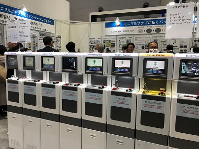
Several new equipment developments were introduced on the show floor. Toray Engineering introduced a bonder for Micro LED mass transfer. Shibuya displayed its latest flip-chip bonder for optical devices. PMT Corp. displayed its “Minimal Fab” for processing WLP and FO-WLP on a small-scale wafer (FIGURE 2). Specialized equipment for molding from Yamada was highlighted in the process.

FIGURE 2. PMT’s Minimal Fab line.
Power devices. Several companies focused on trends in power device and packaging. Rohm discussed SiC for power devices, and Japan’s National Institute of Advanced Industrial Science and Technology (AIST) described the development of SiC super junction Mosfet with extremely low on-resistance. STMicroelectronics also presented power device developments. Senju Metal and Heraeus described materials targeted for power semiconductors.
AI IoT smart homes. AIoT Cloud and Daiwa Connect described how AI and IoT are increasingly combined. AIoT Cloud is a new company developing AIoT conversion of Sharp’s appliances. Areas of focus include making data usable for cooking, washing clothes, air-conditioning, and air purification. Daiwa provided examples, including smart homes with special emphasis on the elderly, intelligent toilets (providing a lot of health information!), and industrial applications.
Toshiba’s keynote described how big data are used to improve yield in the factory. While data collection is important, the key is using systems instead of humans for analysis and decision-making. Examples of machine learning to identify the types and causes of defects were presented. The automation of yield analysis requires input from many sensors such as flow rate, pressure, measurements. Capturing the data with machines is possible for 90% of the information needed today, but humans are still required.
Pervasive 5G theme. Many presentations discussed 5G, including use conditions that can help monetize investment in the infrastructure. Qualcomm discussed material innovations required for 5G packages. The discussion focused on the need for low Dk/Df substrate dielectrics, low Dk/D mold compounds, and the need for conformal shielding overmold and substrate sidewalls, as well as the use of electrically conductive paste. Qualcomm highlighted its AiP module, digital module for the application processor and modem, and its radio frequency (RF) front-end (FE) module.
One session discussed the requirements for substrate materials as the industry moves to 6G, with presentations from AGC and Oki. Semi Consult discussed flex circuits for 5G mobile phones, highlighting Apple’s iPhone.
PCB materials. Hitachi Chemical and Zhen Ding Technology (ZDT) discussed new materials and processes for PCBs. A presentation from Robert Bosch described the impact of autonomous driving and electrification on the PCB and its reliability requirements. Challenges of miniaturization, higher frequencies, and new high-speed materials with high temperatures are creating manufacturing, reliability, and testing challenges. Meiko Electronics described 5G material trends and challenges, such as transmission loss by the PCB material and copper foil surface, and RF material.
Next year’s conference will take place from Jan. 20-21 at Tokyo Big Sight. The conference will be combined again with Robotics, Wearables, and SmartFactory.
is president of TechSearch International (techsearchinc.com); jan@techsearchinc.com; @jan_techsearch.


