

Benefits and Challenges of 3D Semiconductor Packaging
Substrate-based IC packaging can adopt a wider range of materials, while accommodating several alternative assembly processes.
The electronics industry is experiencing a renaissance in semiconductor package technology. This is due to the growing number of innovative 3D package assembly solutions that have evolved to further enable product functionality without increasing product size. Multiple die packaging commonly uses a substrate interposer as a base. By integrating multiple die elements within a single package outline, overall product functionality has increased and been made smaller than their predecessors, improving both performance and capability. Assembly of semiconductor die onto a substrate is essentially the same as those used for standard IC packaging in lead frames; however, substrate-based IC packaging for 3D applications can adopt a wider range of materials, and several alternative processes may be used in their assembly.
Companies that have already implemented 3D semiconductor packaging have experienced success in both stacked die and stacked package methodology. Although 3D package technology has reached a level of maturity, there remain a number of issues to consider when selecting the specific methodology to be used in developing a multiple die package. The platform for mounting the die is typically one of three material sets: alumina (ceramic); a high Tg glass reinforced epoxy laminate; and, for less complex applications, one and two metal layer polyimide films. Because of the relatively high I/O required to interface multiple die, the interposers commonly adopt a uniform array configured ball or bump contact design. Limiting the semiconductor package size continues to be a factor; however, the package outline will always be controlled by the size of the largest die and number of interface contacts. The base structure (interposer) selected must furnish a surface area large enough to enable the wire-bond operation and be mechanically stable enough to withstand the process temperatures of the entire package assembly process (die attach, wire-bond and encapsulation).
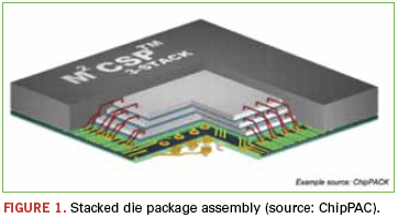
Die stack assembly. When vertically stacking two or more semiconductors for wire-bond assembly, the die elements will ideally have a progressively smaller outline. This “tiered” configuration permits all die to be sequentially attached on top of one another in a single operation, leaving the edge of die elements accessible for the subsequent wire-bond operation (Figure 1). A tiered die format will generally furnish the lowest overall multiple die package profile. There also is potential for improving package performance due in part to the very short coupling between vertically configured semiconductor die. Because they generally utilize a common interposer, the package typically exhibits lower inductance and reduced overall power consumption.
When the die outlines are the same size or near the same, spacers are added between each die to clear the wire-bond features. The basic process of assembly of same size die is not unlike the tiered variation, but die attach and wire-bond operations must be performed sequentially. That is, each die is individually attached and wire bonded to the base substrate before adding a spacer and the next die in the stack and so on. Due to the limited space between die elements, conventional wire-bond loop height may not be low enough to overcome the potential interference between the bond wire profile and next-level die. Companies will often resort to a reverse-bond process typical of that shown in Figure 2. Although the die and spacer assembly method is widely used for packaging memory die, the increased complexity of the sequential stacking process does significantly impact the overall throughput efficiency for package assembly. 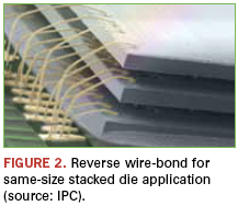
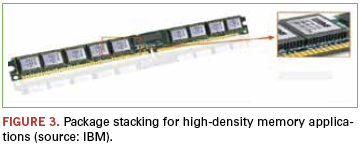
Package stacking. Vertically mounting one or more packaged die (package-on-package) has evolved as a preferred alternative to die stacking for a growing number of applications. The package stacking process was initially adopted by memory semiconductor companies to provide a simple solution for furnishing significantly higher density configurations to keep pace with the more advanced processors. For DRAM applications with center located bond pads, the die element is mounted face-down on an organic interposer that is slightly wider than the die element to accommodate solder ball contacts. The wire-bond interface between the die and interposer is made from the bottom surface of the interposer followed by encapsulation, solder ball attach and test. The module configuration in Figure 3 exhibits four vertically mounted DRAM die package sections, using only the edge-located solder ball contacts for mechanical and electrical interface.
Developing a multiple die, system level package with related but dissimilar functions within a single package outline will enable greater PCB surface utilization and potentially provide enhanced electrical performance. In reviewing a typical system application for a personal GPS product (Figure 4), it is apparent a number of candidate semiconductor functions could be integrated into a common 3D package configuration. To minimize product size and optimize the PCB area utilization, it is conceivable to combine a number of closely related functions into four or five package-on-package assemblies.
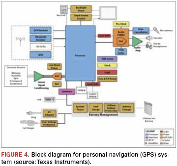
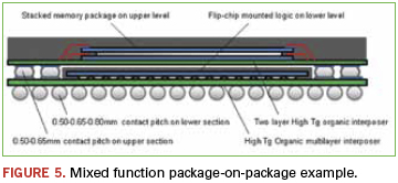
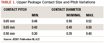
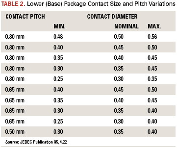
A likely configuration for package stacking would begin with the processor die element packaged onto the base substrate. This processor die will have significantly more I/O than any other closely related semiconductor functions may be mounted face-up for wire-bond assembly or (after wafer level redistribution and bumping) mounted face-down for direct solder attachment. The second-level package layer will most likely furnish the memory functions. In the GPS instance, for example, SDRAM and FLASH/ EPROM functions are directly interfaced with the processor units. Packaging memory using the die stack process described above is preferred for the upper section because wafer level fabrication, when mature, is a high yield process. The lower-packaged processor, on the other hand, is most often packaged solo because the processor will require very specialized electrical test methodology before joining the sections. The example in Figure 5 illustrates the now familiar package-on-package configuration for mixed function applications. The JEDEC-defined ball contact pitch and diameter variations developed for each section of the package-on-package family are furnished in Table 1 and Table 2.
Other candidates for 3D packaging on the GPS example include the RF/IF components, the display drivers, audio, power management and signal conditioning elements. They may be packaged using either die stack or package stack or a combination of both, depending on die level yields and electrical test complexity.
Although the benefit gained with 3D semiconductor packaging is very high, a number of challenges will need to be addressed. In addition to selecting a competent supplier for package assembly and test, users need to consider the reliability of the supply chain for the die elements selected. Further, before performing assembly, whether stacking die or stacking packaged die, the package assembly specialist often will want to reduce the die elements’ thickness. Thinning of the individual die units contributes to process uniformity and enables the reduction in overall package height. The thinning process, however, is performed while the die elements remain in the wafer format. Some semiconductor suppliers are reluctant to furnish full wafers to outside sources, though, because the thinned wafers are more difficult to transport. Additionally, if die elements are supplied to the assembly service company already singulated, the fabricator may be reluctant to perform any special thinning services that may affect yield.
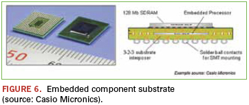
Embedded components. The process for embedding components in the PCB substrate is not new, but semiconductor companies are now adopting the methodology in high volume using wafer-level operations they refer to as “fan-out WLP.” All the packaging operations are performed sequentially at the wafer level. Additional area must be provided to extend the package size beyond the IC surface area to allow for increased solder ball population and a contact pitch more suitable for conventional SMT assembly processing. The die element embedded within the substrate interposer’s “core” section (Figure 6) is a relatively robust 150µm in thickness, but many companies are thinning die down to 50µm to further minimize substrate thickness. In regard to the SMT ball pitch furnished for assembly, 0.50mm has been the norm for a majority of the array configured components, but 0.40mm ball pitch is not uncommon.
Package performance. Designers are well aware that the shorter the circuit interface provided between the individual die elements, the greater the signal transmission speed. By embedding the semiconductor on an innerlayer directly in line with a related semiconductor package mounted on the outer surface, the conductor interface can be minimized. With the die element mounted within or onto the substrate interposer’s core layer, resin-coated foil is laminated over the area to enable circuit interface to the layers above. The interface is made through small microvias that are laser ablated and plated directly to the bond-sites of the die element. Additional RCC layers are built up on the substrate’s base sequentially to complete the interface to the outer surface layers of the interposer. When die elements are prepared with bump contacts, the die can be mounted face down onto a mating contact pattern for solder or conductive polymer attachment. Several PCB suppliers with experience in buildup circuits are involved in embedding both passive and active components. A majority of companies furnishing embedded component substrates in high volume are located in Europe and Asia, but there are number of capable North American suppliers as well.
Concerns
Testing 3D die-stacked packages with mixed function die has been a serious defector because of the unique testing requirements of dissimilar functions. Combining logic functions with memory in a single package outline, for example, has always proven difficult. This is because testing and burn-in requirements for memory devices are very different than that required for the logic functions. Additionally, when several functionally different die elements are stacked within a single package outline (die-stack), the differences in die sizes and the die quality can adversely affect package assembly yields. Package-on-package products, on the other hand, permit functional test of each section before joining. Test before joining has proved far more practical both for suppliers and users because the sections can be supplied as separate units and joined at the board-level assembly stage, or furnished as a single package-level product, thoroughly tested and certified to be ready for PCB mounting.
PCB assembly issues. Users of the PoP product have experienced a number of challenges. The multiple level package families, when furnished on an organic substrate, are more sensitive to the effects of the thermal profile developed for reflow solder attachment. Users have experienced excessive warping of the package substrate sections, typically occurring during reflow solder heating. As the substrate temperature exceeds the point of glass transition, the rigid resin-based laminate relaxes somewhat, permitting the material to reach a condition that can result in deformation. The deformation is most prominent at the outer edge area and corners of the substrate sections. When the warping results in the substrate deforming away from the circuit board surface, solder joints can elongate or separate from the opposing surface. When the substrate warps downward at the edge or corner areas, the contacts will compress, often forming a common connection or short between adjacent contact sites. Both conditions can be avoided by refining the reflow solder profile. The temperature level and timing is dependent on individual assembly complexity and the specific reflow oven used. Many have found, however, that when the materials are exposed to a gradual thermal rise through the solder’s liquidus threshold and peak temperature, substrate warping is minimal and self-correcting.
Embedded component process issues. When producing an organic substrate for the package, module or unit, a reliable infrastructure must be in place to accommodate the manufacturing processes. One key issue is ownership, especially for the embedded active die elements. Due to the number of process steps involved throughout the embedded component fabrication operations, the component parts will be subject to damage. Ideally, the originating companies will bring together the two primary suppliers: the circuit board fabricator and the contract electronics assembler. Some companies may have already established both these capabilities, but others will need to develop partnerships. These partnerships must be willing to adjust their portion of the generated revenue against the overall process yield. That will include sharing losses from fabrication process defects and damaged components.
Economics
Economics has a significant influence on key materials used in 3D semiconductor packaging. The primary element affecting package cost is the substrate interposer. Because of the relative complexity of the newer generations of high-performance semiconductors, I/O counts are expanding. To control the outline limits of the die element, semiconductor designers are reducing the wire-bond contact pitch to less than 50µm. To prepare the die for flip-chip mounting and enable surface area on the substrate for efficient circuit routing, the wire-bond contact sites must be redistributed to a more uniform array format. Flip-chip configured die are commonly furnished with contact spacing in a range from 0.50 to 0.40mm pitch. These contact sites are generally furnished with a raised, solder-compatible bump, sphere or post feature for reflow solder attachment. As the array contact pitch approaches 0.35 and 0.30mm, however, conventional placement and solder attachment methods will be more difficult. Three types of interconnects are currently in use for very-fine pitch flip-chip die: high-Pb alloy bump, Pb-free bump and copper post. The high-Pb bump is being phased out due to RoHS requirements, and Pb-free bump is somewhat limited due to solder collapse. Additionally, the widely used SnAgCu alloy composition is prone to void formation due to electromigration.
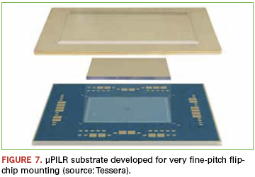
The copper-post-on-die contact has evolved as a viable solution for a number of high-performance semiconductor applications because it enables very-fine pitch (<0.40mm) capability. Some issues with copper-post-on-die, however, are the relatively high cost of wafer level processing and uncertain physical integrity, especially when mounted onto extremely low-k dielectrics. The typical failure mode seen in all of these very fine-pitch flip-chip interconnects is related to solder joint fatigue, cracking and voiding in the solder interface. Voiding is often due to the effects of electromigration, a result of long-term exposure to high current densities. An alternative substrate interconnect solution has been developed to address these troubling product reliability issues, while offering a roadmap to fine-pitch flip-chip contact spacing well below 100µm. The µPILR substrate (Figure 7) was developed for one of the new generations of high-end processors. The substrate has an array of 10,132 solid copper pillars on 150µm and 200µm pitch. In this example, the solid copper µPILR contact features are integrated onto a 10 layer (3-4-3) organic substrate structure that measures 40 x 40 x 1.2mm thick.
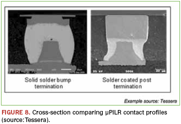
Because the contact formation is part of the substrate fabrication process and manufactured using conventional industry equipment and materials, additional cost for furnishing the raised contact array is minimal. Depending on the method of manufacturing, these interconnects can be furnished in different sizes (diameter and height) and shapes. Furthermore, the flip-chip to µPILR substrate assembly process requires no special consideration beyond that normally used for mounting very-fine-pitch configured die. Because the solid copper contacts are NiAu-plated, a flip-chip configured semiconductor die with either solid solder bump or solder alloy coated copper post contacts will enable a uniform and reliable solder joint (Figure 8). In regard to the effects of electromigration, the µPILR contact has exhibited no significant voiding or cracking in the solder interface, even when exposed to high current density conditions.
Note: µPILR is a trademark of Tessera Inc. or its affiliated companies in the US and other countries.
Vern Solberg is an independent consultant specializing in SMT and microelectronics design and manufacturing technology; vsolberg123@aol.com.


Press Releases
- Altus Adds LPKF CuttingMaster 3290 to Depaneling Portfolio
- Kurtz Ersa Partners with E-tronix for Sales in Illinois and Wisconsin
- XLR8 EMS Welcomes Raul Jorge Lopez Jr. as Director of Program Management and Procurement
- Koh Young America Promotes Ramiro Mora to Lead Service and Applications in Mexico and South America